Liquid crystal display panel

A liquid crystal display panel and color film substrate technology, which is applied in nonlinear optics, instruments, optics, etc., can solve problems such as difficult control of gaps, poor contact between metal wires and external output pins, and influence on the display effect of liquid crystal display devices. The effect of increasing the electrical contact area and improving the bonding yield

Active Publication Date: 2020-03-17
SHENZHEN CHINA STAR OPTOELECTRONICS TECH CO LTD
View PDF11 Cites 19 Cited by
  • Summary
  • Abstract
  • Description
  • Claims
  • Application Information

AI Technical Summary

Problems solved by technology

However, the side bonding technology has the problem that the gap between the array substrate and the color filter substrate on the side where the chip-on-chip film is bonded is difficult to control, resulting in poor contact between the metal wire and the external output pin, which affects the display effect of the liquid crystal display device.

Method used


Image

  • Liquid crystal display panel
  • Liquid crystal display panel
  • Liquid crystal display panel

Examples


Embodiment Construction

[0024] The technical solutions in the embodiments of the present application will be clearly and completely described below in conjunction with the drawings in the embodiments of the present application. Apparently, the described embodiments are only some of the embodiments of this application, not all of them. Based on the embodiments in this application, all other embodiments obtained by those skilled in the art without making creative efforts belong to the scope of protection of this application.

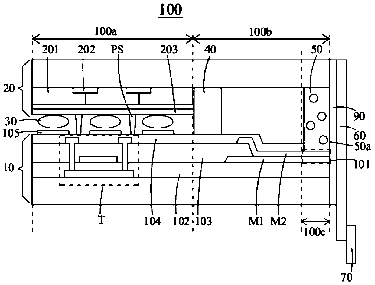
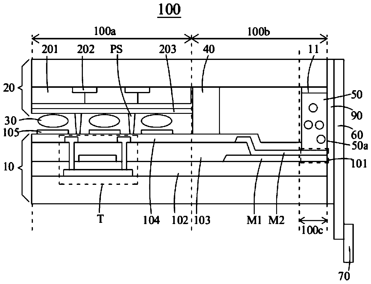
[0025] see figure 1 , which is a schematic diagram of the first structure of the liquid crystal display panel of the embodiment of the present application. The liquid crystal display panel 100 may be one of a twisted nematic liquid crystal display panel, a plane switching liquid crystal display panel or a vertical alignment liquid crystal display panel. Specifically, the liquid crystal display panel 100 is a twisted nematic liquid crystal display panel or a vertical alignment l...


PUM

PropertyMeasurementUnit
widthaaaaaaaaaa
widthaaaaaaaaaa
particle diameteraaaaaaaaaa

Abstract

The invention provides a liquid crystal display panel. The conductive frame adhesive is arranged between a plurality of terminals of an array substrate and a color film substrate, chip-on films are bound on side surfaces of the conductive frame adhesive and terminals in the thickness direction so as to increase the electrical contact area when the chip-on films are bound, and thereby the binding yield of the chip-on films is improved.

Description

technical field [0001] The present application relates to the field of display technology, in particular to a liquid crystal display panel. Background technique [0002] In recent years, with the constant development of the liquid crystal display (Liquid Crystal Display, LCD) display industry, the appearance of the liquid crystal display panel tends to become narrower gradually. For example, narrow-frame TVs and full-screen mobile phones narrow the non-display area at the edge of the liquid crystal display device to increase the area of ​​the display area and increase the screen-to-body ratio. The product is more beautiful. [0003] At present, side bongding (Side bongding) technology can be used to achieve a narrow bezel of less than 1 mm in a liquid crystal display device. The side bonding technology is to print metal wires on the side of the array substrate and make the metal wires electrically contact with the Outer Lead Bonding pad (OLBpad) on the array substrate side...

Claims


Application Information

Patent Timeline
Patent Type & Authority Applications(China)
IPC IPC(8): G02F1/1345G02F1/1339
CPCG02F1/13452G02F1/1339
Inventor 周凯锋
Owner SHENZHEN CHINA STAR OPTOELECTRONICS TECH CO LTD
Why Eureka
Try Eureka