Silicon carbide PiN diode with buried layer structure

A silicon carbide and diode technology, applied in electrical components, circuits, semiconductor devices, etc., can solve the problems of reducing diode on-resistance, small forward current, reducing on-state loss, etc., to improve forward on-current and enhance the effect. , Improve the effect of forward conduction performance

Active Publication Date: 2020-02-28
UNIV OF ELECTRONICS SCI & TECH OF CHINA
View PDF4 Cites 0 Cited by
  • Summary
  • Abstract
  • Description
  • Claims
  • Application Information

AI Technical Summary

Problems solved by technology

[0004] Aiming at the problem of small forward current of traditional silicon carbide PiN diodes, the present invention proposes a silicon carbide PiN diode with a buried layer structure, by introducing a P-type buried layer 5 so that the P-type region 6 and the N-type silicon carbide epitaxial layer 4 The electric field at the boundary is enhanced. By introducing the N-type buried layer 3, the electric field at the boundary between the N-type silicon carbide substrate and the N-type silicon carbide epitaxial layer 4 is enhanced. Compared with the traditional silicon carbide PiN diode structure, the present invention is in the forward conduction It has a stronger conductance modulation effect, reduces the on-resistance of the diode, reduces its on-state loss, and improves the forward characteristics of the SiC PiN diode.

Method used


Image

  • Silicon carbide PiN diode with buried layer structure
  • Silicon carbide PiN diode with buried layer structure
  • Silicon carbide PiN diode with buried layer structure

Examples


Embodiment Construction

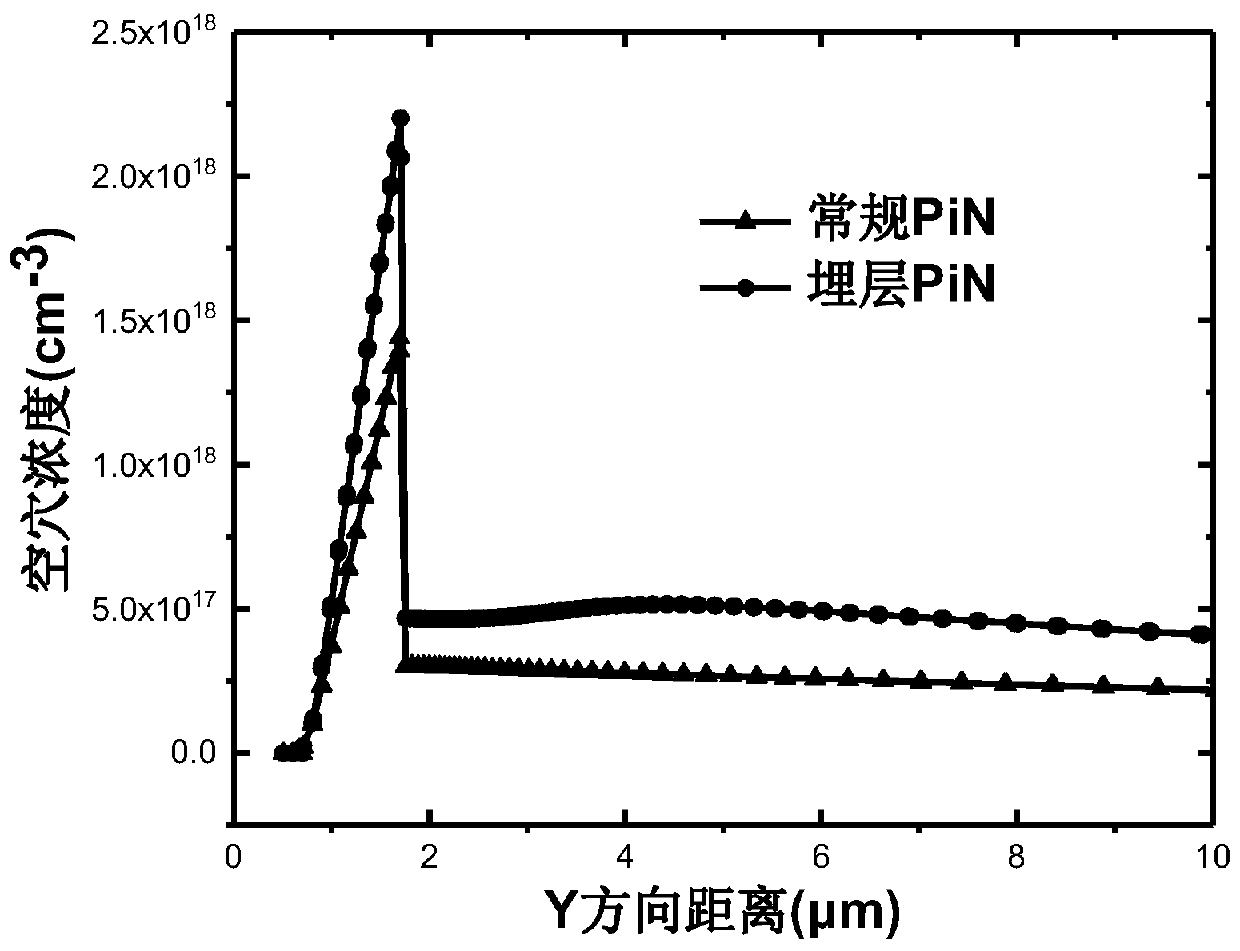
[0016] The advantages of the silicon carbide PiN diode with buried layer structure of the present invention will be further described by way of examples, simulation and description of drawings.

[0017] Such as figure 1 As shown, a silicon carbide PiN diode with a buried layer structure proposed by the present invention includes an N-type silicon carbide substrate 2, a cathode 1 is connected to the lower end of the N-type silicon carbide substrate 2, and a cathode 1 is connected to the upper end of the N-type silicon carbide substrate 2. The N-type silicon carbide epitaxial layer 4, the upper surface of the N-type silicon carbide epitaxial layer 4 is provided with a P-type region 6, and a metal anode 7 is connected above the P-type region 6, and the P-type region 6 forms an ohmic contact with the metal anode 7.

[0018] The present invention proposes to set only N-type buried layer 3 in N-type silicon carbide epitaxial layer 4, or only set P-type buried layer 5 in N-type silic...


PUM

PropertyMeasurementUnit
thicknessaaaaaaaaaa
thicknessaaaaaaaaaa

Abstract

A silicon carbide PiN diode with a buried layer structure comprises a cathode, an N-type silicon carbide substrate, an N-type silicon carbide epitaxial layer, a P-type region and a metal anode which are sequentially arranged from bottom to top. An N-type buried layer and/or a P-type buried layer are/is further arranged in the N-type silicon carbide epitaxial layer. The N-type buried layer is located above the N-type silicon carbide substrate and used for enhancing the electric field at the boundary of the N-type silicon carbide substrate and the N-type silicon carbide epitaxial layer. The P-type buried layer is located below the P-type region and used for enhancing the electric field at the boundary of the P-type region and the N-type silicon carbide epitaxial layer. According to the invention, the P-type buried layer is introduced to enhance the electric field at the boundary of the P-type region and the N-type silicon carbide epitaxial layer, and the N-type buried layer is introducedto enhance the electric field at the boundary of the N-type silicon carbide substrate and the N-type silicon carbide epitaxial layer, so that the conductivity modulation effect is enhanced, the forward conduction current of the silicon carbide PiN diode is improved, and the forward conduction performance of the silicon carbide PiN diode is improved.

Description

technical field [0001] The invention belongs to the technical field of power semiconductor devices and relates to a silicon carbide PiN diode with a buried layer structure. Background technique [0002] Wide bandgap semiconductor material silicon carbide (SiC) has the advantages of wide bandgap width, high critical breakdown electric field, high thermal conductivity, high electron saturation rate and good thermal stability. Ideal material for semiconductor devices under strong radiation environment. Under the same conditions, silicon carbide PiN diodes have higher breakdown voltage and lower on-state resistance than silicon PiN diodes. The performance improvement of silicon carbide PiN diodes is due to its superior material properties: high critical breakdown electric field can make the drift region of silicon carbide PiN diodes thinner, and the doping is correspondingly larger, which not only reduces the forward conduction resistance At the same time, the switching speed ...

Claims


Application Information

Patent Timeline
Patent Type & Authority Applications(China)
IPC IPC(8): H01L29/868H01L29/16H01L29/06
CPCH01L29/0684H01L29/1608H01L29/868
Inventor 王帅张有润罗佳敏钟炜罗茂久
Owner UNIV OF ELECTRONICS SCI & TECH OF CHINA
Why Eureka
Try Eureka