
Diode chip of integrated unit

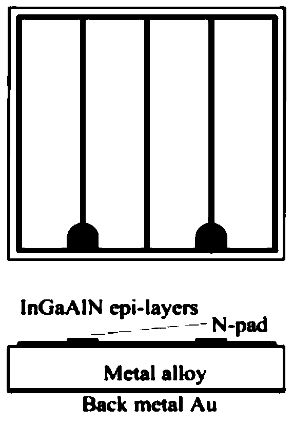
A technology of integrated units and diodes, applied in electrical components, electrical solid devices, circuits, etc., can solve problems such as LED light efficiency, heat dissipation and stability limitations, and achieve increased effective light output area, large heat dissipation area, and high photoelectric conversion efficiency Effect

Active Publication Date: 2020-02-14
SOUTH UNIVERSITY OF SCIENCE AND TECHNOLOGY OF CHINA
View PDF14 Cites 1 Cited by
  • Summary
  • Abstract
  • Description
  • Claims
  • Application Information

AI Technical Summary

Problems solved by technology

Therefore, LED light efficiency, heat dissipation and stability under high current will be severely limited

Method used


Image

  • Diode chip of integrated unit
  • Diode chip of integrated unit
  • Diode chip of integrated unit

Examples


Embodiment 1

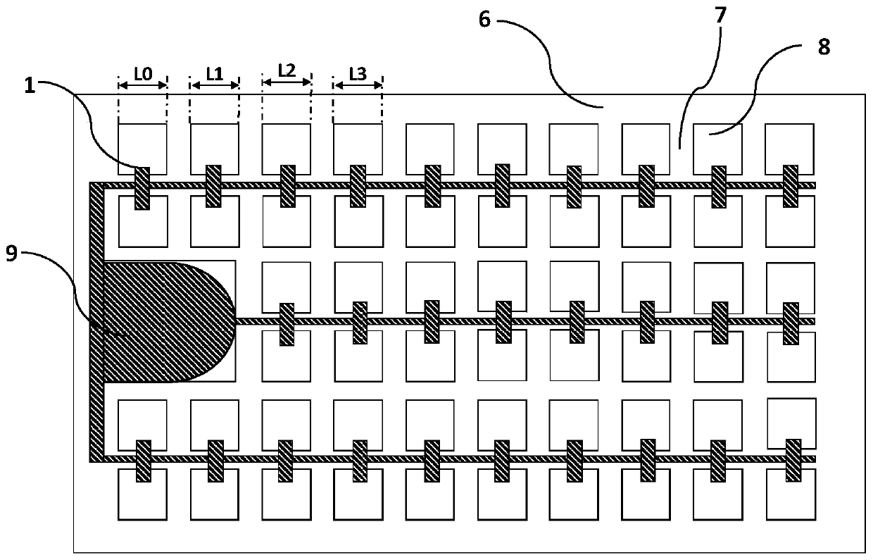
[0029] The present embodiment provides 3 kinds of uniform light-emitting integrated unit diode chips, such as Figure 3-5 As shown, it includes a second conductivity type electrode 1 , a diode mesa structure 6 located on the first conductivity type electrode, a trench structure 7 , and a second conductivity type pad 9 . The diode mesa structure includes a plurality of diode units 8 arranged in a geometric shape, the diode units are connected in parallel, and the area of ​​the mesa structure is determined according to the current diffusion length. Wherein the second conductivity type electrode 1 is an n electrode, and the second conductivity type pad 9 is an n pad.

[0030] Such as image 3 As shown, the diode mesa structure includes 56 square diode units in 6 rows and trench structures 7, and the trench structures are located between the diode units. The diode units are uniformly distributed in the mesa structure, and the length of the diode units along the x-axis direction ...

Embodiment 2

[0037] This embodiment provides two kinds of uniform light-emitting integrated unit diode chips, as shown in Figures 6-7, including a second conductivity type electrode 1, and a diode mesa structure 6 on the first conductivity type electrode with a second conductivity type Type Pad 9. The diode mesa structure includes a plurality of diode units 8 arranged in a geometric shape, the diode units are connected in parallel, and the area of ​​the mesa structure is determined according to the current diffusion length. Wherein the second conductivity type electrode 1 is an n electrode, and the second conductivity type pad 9 is an n pad.

[0038] Such as Figure 6 As shown, the diode mesa includes 6 rows of 26 equal-sized square diode units and trench structures 7, each diode unit has a width of 1 micron to 100 microns along the y-axis direction, and the diode units with trench structures are evenly distributed On the left side of the mesa structure, on the right side of the mesa str...


PUM

PropertyMeasurementUnit
Diameteraaaaaaaaaa

Abstract

The invention provides a diode chip of an integrated unit. The diode chip includes a diode mesa structure, including a plurality of diode units. The width of the diode units in the y-axis direction gradually decreases from the middle to both sides of the integrated unit diode chip in the y-axis direction, wherein the y-axis direction is the width direction of the integrated unit diode chip. Through the design of the uneven mesa structure, ultra-uniform current distribution, heat distribution, wavelength distribution and a high-quality LED light source with narrow half-height are obtained; thetechnical problem that a diode structure in the prior art has great limitations on three important parameters of lumen efficiency, lumen density output and lumen cost is solved; lumen output per unitarea of the chip is improved; and lumen cost is reduced.

Description

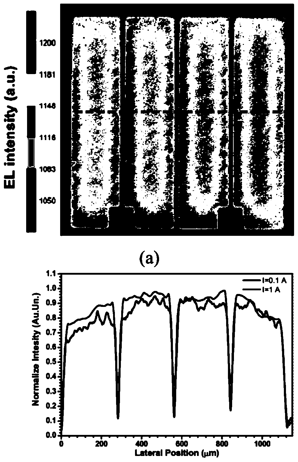
technical field [0001] The invention relates to the field of semiconductor materials and device technology, in particular to semiconductor optoelectronic devices. Background technique [0002] In conventional vertical structure LED chips, the current diffusion mainly depends on the n-electrode side, and there are electrode lead-type leads or drill-type leads, but the overall current diffusion is still uneven, resulting in loss of luminous efficiency and uneven heat dissipation, thus affecting the unit. Efficiency and stability of diode chips. This restricts vertical high-power LED chips from providing products with higher lumen output per unit area. Uneven current diffusion, uneven thermal diffusion, and uneven light extraction lead to great limitations in the three important parameters of lumen efficiency, lumen density output, and lumen cost. The vertical LED chip technology currently on the market An effective solution cannot be provided. [0003] The prior art one is ...

Claims


Application Information

Patent Timeline
IPC IPC(8): H01L27/15H01L33/20
CPCH01L27/156H01L33/20
Inventor 蒋振宇闫春辉
Owner SOUTH UNIVERSITY OF SCIENCE AND TECHNOLOGY OF CHINA
Learn More