Semiconductor memory

A memory and semiconductor technology, applied in semiconductor devices, electric solid state devices, transistors, etc., to avoid short circuits between bit line contacts and side erosion problems

Pending Publication Date: 2020-02-14
CHANGXIN MEMORY TECH INC
View PDF0 Cites 2 Cited by
  • Summary
  • Abstract
  • Description
  • Claims
  • Application Information

AI Technical Summary

Problems solved by technology

[0004] The main purpose of this application is to provide a manufacturing method and structure of a memory bit line, to solve or alleviate one or more technical problems in the prior art, and at least provide a beneficial option

Method used


Image

  • Semiconductor memory
  • Semiconductor memory
  • Semiconductor memory

Examples


Embodiment approach 1

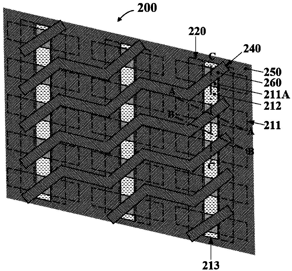
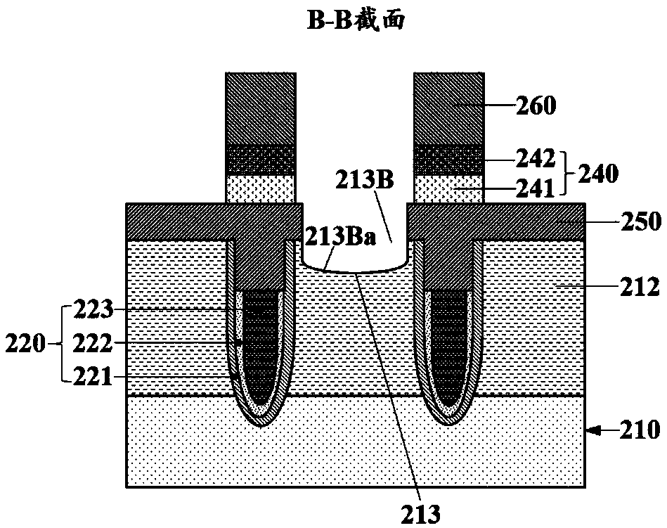
[0121] The present invention provides a semiconductor memory structure, including: a substrate 210, a word line 220, a bit line contact 230, a bit line 240, a protective layer 250 and a first barrier layer 260, such as Figures 1a-1d shown.

[0122] Wherein, the upper surface of the substrate 210 defines a plurality of active regions 211, and the active regions 211 are arranged at intervals to form an active region array, and the active regions 211 are formed on the surface of the substrate 210 and do not penetrate the substrate 210, such as Figure 1a , 1b shown. In one embodiment, the material of the active region 211 includes doped Si.

[0123] An isolation structure 212 is disposed between the active regions 211, and the isolation structure 212 is formed in the substrate 210 and insulates the active regions 211 from each other, such as Figure 1a , 1c . In one embodiment, the isolation structure 212 may be shallow trench isolation (Shallow Trench Isolation, STI), and th...

Embodiment approach 2

[0136] Another embodiment of the present invention selects different etchant gases in order to further reduce SiO 2 The etch selectivity ratio of / Si and the re-recess depth of the inter-window groove 213B.

[0137] A semiconductor memory structure, comprising: a substrate 210, a word line 220, a bit line contact 330, a bit line 240, a protection layer 250 and a first barrier layer 260, such as Figures 4a-4d shown.

[0138] Wherein, the upper surface of the substrate 210 defines a plurality of active regions 311, the active regions 311 are arranged at intervals to form an active region array, the active regions 311 are formed on the surface of the substrate 210 and do not penetrate the substrate 210, as Figure 4a , 4b shown. In one embodiment, the material of the active region 311 includes doped Si.

[0139] An isolation structure 312 is disposed between the active regions 311, and the isolation structure 312 is formed in the substrate 210 and insulates the active region...


PUM

PropertyMeasurementUnit
thicknessaaaaaaaaaa
thicknessaaaaaaaaaa

Abstract

The invention provides a semiconductor memory structure, which comprises a substrate, word lines, bit line contacts and bit lines, and is characterized in that a through channel is formed between every two adjacent word lines, each channel comprises a contact window and an inter-window groove, each inter-window groove is provided with a re-recessed surface relative to the contact window, and the re-recessed depth ranges from 5.8nm to 8.5nm, so that the adjacent bit line contacts are not electrically connected with each other; and the sum of the side etching depths of the bit line contact is indirect proportion to the re-recessing depth of the inter-window grooves in the extension direction of the word lines. The invention further provides another semiconductor memory structure, which is characterized in that the contact window in the channel is provided with a re-recessed surface relative to the inter-window groove, and the re-recessed surface is lower than the surface of an isolationstructure in the channel; and each bit line contact has a vertical sectioning profile in the extension direction of the word lines. By controlling the proportion of the etching agent gas or selectingdifferent etching agents, the problem of serious side etching of the bit line contacts due to the formation of the relatively low re-recessed surface of the inter-window grooves is effectively solved.

Description

technical field [0001] The invention relates to the field of semiconductor integrated circuits, in particular to a semiconductor memory structure and a manufacturing method thereof. Background technique [0002] A semiconductor memory generally includes a plurality of memory cells and word lines and bit lines connected to the memory cells. During the manufacturing process of the bit line, it is necessary to over-etch the protective layer between two adjacent word lines to fully expose the underlying active region and isolation structure, so as to form a bit line contact window. Usually, the same etchant is used to etch the protective layer, the active region and the isolation structure together. Due to the etchant on the active region (such as Si) and the isolation structure (such as SiO 2 ) has a difference in etching selectivity, which makes it easy to form trenches on the surface of the isolation structure. When the trench is deep, more material of the bit line contact...

Claims


Application Information

Patent Timeline
Patent Type & Authority Applications(China)
IPC IPC(8): H01L27/108
CPCH10B12/30H10B12/485
Inventor 不公告发明人
Owner CHANGXIN MEMORY TECH INC
Why Eureka
Try Eureka