Free ground film, circuit board and preparation method of free ground film

A printed circuit board, free technology, applied in the field of electronics, can solve the problems of affecting the signal transmission of the circuit board, unable to interfere with the export of charges, the connection failure between the free grounding film and the electromagnetic shielding film, etc., to achieve the effect of ensuring integrity and grounding

Pending Publication Date: 2020-02-11
GUANGZHOU FANGBANG ELECTRONICS
View PDF0 Cites 0 Cited by
  • Summary
  • Abstract
  • Description
  • Claims
  • Application Information

AI Technical Summary

Problems solved by technology

However, in the process of implementing the present invention, the inventors found that there are at least the following problems in the prior art: at high temperature, due to the expansion of the conductive adhesive layer, the conductive particles in the conductive adhesive layer that were originally in contact with each other will be pulled apart or the conductive particles that were originally in contact with each other will be separated. The conductive particles in contact with the electromagnetic shielding film are pulled apart, resulting in the failure of the connection between the free grounding film and the electromagnetic shielding film, so that the interference charges accumulated on the electromagnetic shielding film cannot be effectively exported, and then form a source of interference, affecting the signal transmission of the circuit board

Method used


Image

  • Free ground film, circuit board and preparation method of free ground film
  • Free ground film, circuit board and preparation method of free ground film
  • Free ground film, circuit board and preparation method of free ground film

Examples


Embodiment 1

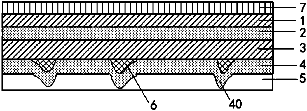
[0055] See figure 1 , the embodiment of the present invention provides a free grounding film, which includes a first conductor layer 1, a conductive adhesive layer 2 and a second conductor layer 3 stacked in sequence, and the second conductor layer 3 is far away from the conductive adhesive layer 2 There is a protrusion 6 on one side;

[0056] The free grounding film also includes a third conductor layer 4 and an adhesive film layer 5, the third conductor layer 4 is arranged on the side of the second conductor layer 3 on which the protrusion 6 is formed, and the third conductor layer A raised portion 40 is formed on the position where the conductor layer 4 covers the raised portion 6 (the relationship between the raised portion 40 and the raised portion 6 can be one-to-one correspondence, one-to-many correspondence or multi-to-one correspondence, etc., when the When the relationship between the raised portion 40 and the raised portion 6 is a one-to-one correspondence, the sha...

Embodiment 2

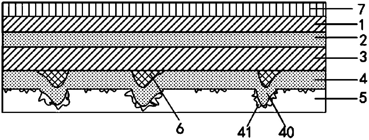
[0078] See figure 2 , this embodiment provides another free grounding film, which differs from the first embodiment mainly in that: the surface of the raised portion 40 is provided with convex conductor particles 41 . Wherein, by arranging the conductor particles 41 on the surface of the raised portion 40, it is further ensured that the raised portion 40 can smoothly penetrate the adhesive film layer 5 and the electromagnetic shielding during the pressing process. The insulating layer 80 of the film 8 further ensures the normal derivation of disturbing charges.

[0079] In the embodiment of the present invention, the height of the conductor particles 41 is preferably 20 μm-100 μm, the thickness of the adhesive film layer 5 is preferably 0.1 μm-80 μm, and the thickness of the insulating layer 80 is preferably 1 μm-20 μm. By setting the height of the conductive particles 41 to preferably 20 μm-100 μm, the thickness of the adhesive film layer 5 is preferably 0.1 μm-80 μm to ens...

Embodiment 3

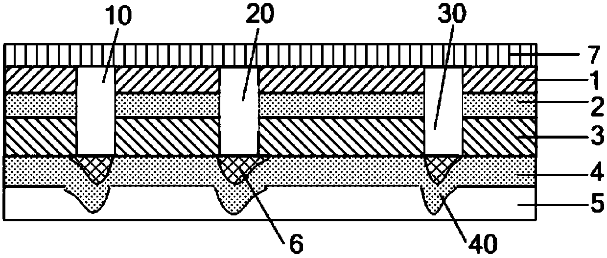
[0085] See image 3 and Figure 5 , this embodiment provides another free grounding film, which differs from Embodiment 1 and Embodiment 2 mainly in that: the formation process of the protrusion 6 is: the first conductor layer 1 is provided with a The first through hole 10 on the surface, the second conductor layer 3 is provided with a second through hole 30 passing through its upper and lower surfaces, and the protrusion 6 is made of fluid resin from the first through hole 10 through the second through hole 30. The conductive adhesive layer 2 is solidified when flowing to the outside of the second through hole 30 .

[0086] Specifically, as image 3 As shown, the protrusion 6 is formed by solidification when the fluid resin flows from the first through hole 10 through the conductive adhesive layer 2 to the outside of the second through hole 30, specifically as follows: The conductive adhesive layer 2 is provided with a third through hole 20 penetrating through its upper an...


PUM

PropertyMeasurementUnit
heightaaaaaaaaaa
thicknessaaaaaaaaaa
thicknessaaaaaaaaaa

Abstract

The embodiment of the invention provides a free ground film, a circuit board and a preparation method of the free ground film. The free ground film includes a third conductor layer, an adhesive film layer, a first conductor layer, a conductive adhesive layer and a second conductor layer, wherein the first conductor layer, the conductive adhesive layer and the second conductor layer are sequentially stacked. The second conductor layer is provided with a protrusion on the side away from the conductive adhesive layer. The third conductor layer is arranged on the side, which is provided with the protrusion, of the second conductor layer. A protrusion part is formed at the site covered by the protrusion on the third conductor layer. The adhesive film layer is arranged on the side, which is awayfrom the second conductor layer, of the third conductor layer. When the free ground film is used for grounding of a printed circuit board, the electromagnetic shielding film is arranged on the printed circuit board. The free ground film and the electromagnetic shielding film are pressed together through the adhesive film layer. The protrusion part penetrates the adhesive film layer and the insulation layer of the electromagnetic shielding film and is electrically connected with the shielding layer of the electromagnetic shielding film. Interference charges accumulated on the shielding layer are effectively led out. An interference source formed by the accumulation of the interference charges is avoided, and thus the integrity of signal transmission is effectively ensured.

Description

technical field [0001] The invention relates to the field of electronics, in particular to a free grounding film, a circuit board and a method for preparing the free grounding film. Background technique [0002] With the rapid development of the electronics industry, electronic products are further developed toward miniaturization, light weight, and high-density assembly, which greatly promotes the development of flexible circuit boards, thereby realizing the integration of component devices and wire connections. Flexible circuit boards can be widely used in industries such as mobile phones, liquid crystal displays, communications and aerospace. [0003] Driven by the international market, functional flexible circuit boards dominate the flexible circuit board market, and an important indicator for evaluating the performance of functional flexible circuit boards is Electromagnetic Interference Shielding (EMI Shielding). With the integration of functions of communication equi...

Claims


Application Information

Patent Timeline
Patent Type & Authority Applications(China)
IPC IPC(8): H05K1/02
CPCH05K1/0218H05K2201/0715
Inventor 苏陟高强朱开辉蒋卫平朱海萍
Owner GUANGZHOU FANGBANG ELECTRONICS
Why Eureka
Try Eureka