CMOS image sensor with time-delay integration and method for forming same

A time-delay integration and image sensor technology, applied in the direction of electric solid-state devices, semiconductor devices, electrical components, etc., to achieve high sensitivity and dynamic range, increase pixel fill factor, and improve performance

Active Publication Date: 2020-02-11
BRIGATES MICROELECTRONICS KUNSHAN
View PDF6 Cites 0 Cited by
  • Summary
  • Abstract
  • Description
  • Claims
  • Application Information

AI Technical Summary

Problems solved by technology

[0005] However, the existing time delay integration CMOS image sensor still needs to improve the performance

Method used


Image

  • CMOS image sensor with time-delay integration and method for forming same
  • CMOS image sensor with time-delay integration and method for forming same
  • CMOS image sensor with time-delay integration and method for forming same

Examples


Embodiment Construction

[0028] As mentioned in the background art, the CMOS image sensor with time delay integration needs to improve its performance.

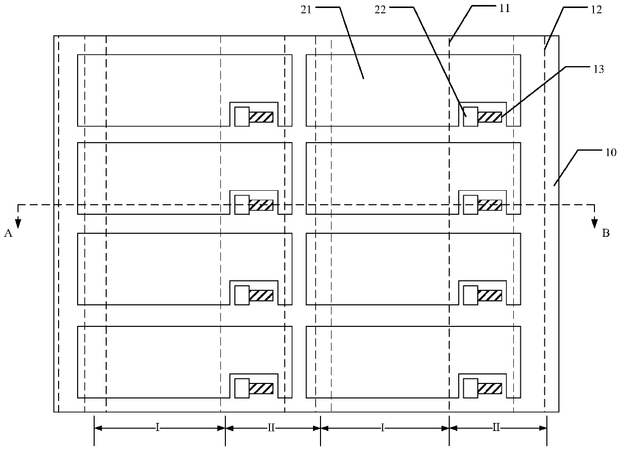
[0029] Under strong light conditions, the phenomenon that the electrons in the channel under the gate structure reach the full well and overflow into the adjacent channel is called the dispersion phenomenon. The dispersion phenomenon will cause the adjacent channels to be crosstalked by charges, resulting in pixels subject to crosstalk. The signal cannot reflect the real illumination, causing the number of saturated pixels to increase than it actually is, resulting in image color distortion, and defects such as halos in the output image, thereby reducing the quality of the output image of the CMOS image sensor with time delay integration.

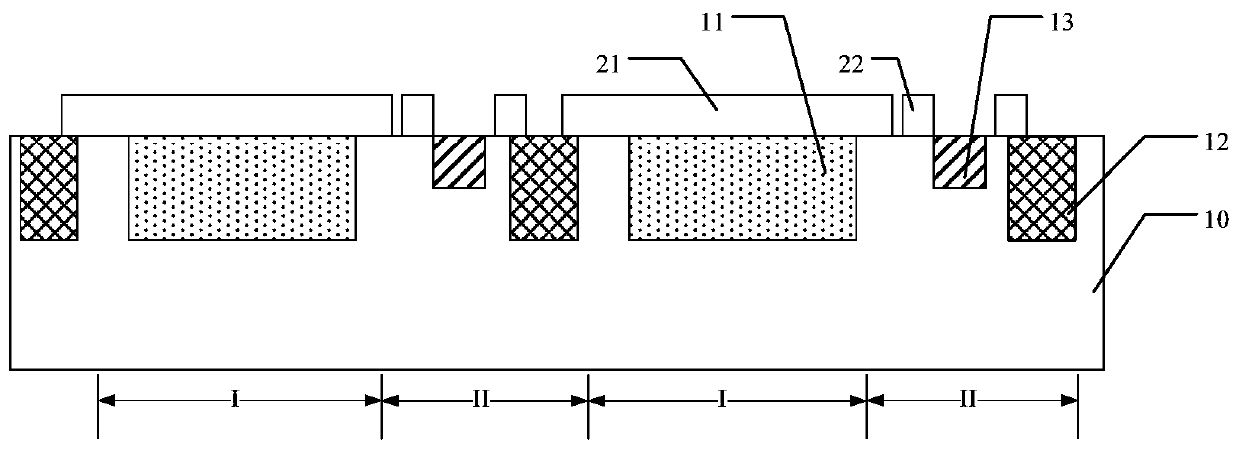
[0030] figure 1 It is a schematic diagram of the top view structure of a CMOS image sensor with time delay integration. figure 2 Yes figure 1 A schematic diagram of the cross-sectional structure along the A-B tangent ...


PUM


Abstract

A CMOS image sensor with time-delay integration and a method for forming the same are disclosed. The CMOS image sensor with time-delay integration includes: a substrate including a plurality of unit regions arranged in a first direction; a first photovoltaic region, a second photovoltaic region, and a source-drain region which are discrete from each other and located in the substrate, wherein thesource-drain region is located between the first photovoltaic region and the second photovoltaic region, and the first photovoltaic region and the second photovoltaic region each stretch across the plurality of unit regions; a first gate structure, a second gate structure, a third gate structure, and a fourth gate structure which are located on the substrate in the cell regions. Therefore, the performance of the CMOS image sensor with time delay integration can be improved.

Description

Technical field [0001] The present invention relates to the field of semiconductors, and in particular to a CMOS image sensor with time delay integration and a forming method thereof. Background technique [0002] Image sensors have been widely used in digital cameras, mobile phones, medical equipment, automobiles and other applications. The rapid development of image sensor technology makes people have higher requirements for the performance of image sensors. [0003] Time Delay Integration (TDI) image sensor is an evolution of linear image sensor. The imaging mechanism of the time delay integral image sensor is to expose the pixels passing by the photographed object line by line, and accumulate the exposure results, thereby solving the problem of weak imaging signal caused by insufficient exposure time of high-speed moving objects. The time delay integral image sensor can increase the effective exposure time and improve the image signal-to-noise ratio. [0004] The time delay in...

Claims


Application Information

Patent Timeline
IPC IPC(8): H01L27/146
CPCH01L27/14614H01L27/14612H01L27/14616H01L27/14689
Inventor 黄金德王林胡万景
Owner BRIGATES MICROELECTRONICS KUNSHAN
Why Eureka
Try Eureka