A kind of bottom filling glue filling method
A technology of bottom filling glue and filling method, which is applied in the direction of semiconductor devices, electrical components, circuits, etc., can solve problems affecting the reliability of packaging, etc., and achieve the effects of improving service life, improving thermal conductivity, and increasing movement speed
- Summary
- Abstract
- Description
- Claims
- Application Information
AI Technical Summary
Problems solved by technology
Method used
Image
Examples
Embodiment 1
[0040] This embodiment provides a method for filling an underfill, including:
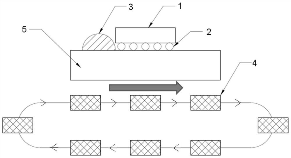
[0041] Add magnetic material to the underfill to form a composite filler 3, which is placed on one side of the chip 1, and the composite filler fills the gap between the substrate and the chip;
[0042] During the filling process, a magnet 4 is placed under the substrate 5 of the electronic packaging device and on the same side of the chip, and the magnet performs a circular movement in the area corresponding to the gap to be filled, and the trajectory is shown in figure 1 , the moving speed of the magnet is 0.5m / s, the magnet drives the magnetic material to move, and then drives the composite filler to flow to the other side of the chip, and fills the gap between the substrate and the chip to complete the filling process;
[0043] At 30°C, a filled electronic packaging device is formed after heating and curing;
[0044] Among them, the composite filler includes bisphenol A epoxy resin and magneti...
Embodiment 2
[0046] This embodiment provides a method for filling an underfill, including:
[0047] Add magnetic material to the underfill to form a composite filler 3, which is placed on one side of the chip 1, and the composite filler fills the gap between the substrate and the chip;
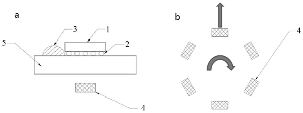
[0048] During the filling process, a magnet 4 is placed under the substrate 5 of the electronic packaging device and on the same side of the chip, and the magnet performs a circular circular motion in the area corresponding to the filled gap, and the movement track of the magnet is shown in figure 2As shown in middle b, the rotation speed of the magnet is 10 μm / s, and the diameter of the circular motion is 30 mm in length of the substrate. The magnet drives the magnetic material to move, and then drives the composite filling glue to flow to the other side of the chip, and the contact between the substrate and the chip is controlled. The gap is filled to complete the filling process;
[0049] At 100°C, af...
Embodiment 3
[0052] This embodiment provides a method for filling an underfill, including:
[0053] Add magnetic material to the underfill to form a composite filler 3, which is placed on one side of the chip 1, and the composite filler fills the gap between the substrate and the chip;
[0054] During the filling process, a magnet 4 is placed under the substrate 5 of the electronic packaging device and on the same side of the chip, and the magnet performs circular motion and centrifugal motion in the area corresponding to the filled gap, and the trajectory is shown in image 3 As shown in middle b, the speed of the circular motion of the magnet is 13 μm / s, and the speed of the centrifugal motion is 3 μm / s. The magnet starts to perform centrifugal motion and circular motion at the center of the substrate, and stops the centrifugal motion when the magnet moves centrifugally to the edge of the substrate. But keep doing the circular motion until the compound filler is completely filled. The m...
PUM
 Abstract
Description
Claims
Application Information
 - R&D
- Intellectual Property
- Life Sciences
- Materials
- Tech Scout
- Unparalleled Data Quality
- Higher Quality Content
- 60% Fewer Hallucinations
Browse by: Latest US Patents, China's latest patents, Technical Efficacy Thesaurus, Application Domain, Technology Topic, Popular Technical Reports.
© 2025 PatSnap. All rights reserved.Legal|Privacy policy|Modern Slavery Act Transparency Statement|Sitemap|About US| Contact US: help@patsnap.com


