Packaging structure

A technology of packaging structure and plastic packaging layer, applied in the direction of semiconductor/solid-state device components, semiconductor devices, electrical components, etc., can solve the problems of poor performance of packaging structure, achieve the effect of improving performance, avoiding collapse, and meeting the requirements of process design

Active Publication Date: 2019-12-24
NANTONG FUJITSU MICROELECTRONICS
View PDF4 Cites 0 Cited by
  • Summary
  • Abstract
  • Description
  • Claims
  • Application Information

AI Technical Summary

Problems solved by technology

[0003] However, the performance of the package structure formed by the existing flip-chip method is poor

Method used


Image

  • Packaging structure
  • Packaging structure
  • Packaging structure

Examples


Embodiment Construction

[0025] As mentioned in the background, the performance of the packaging structure formed by the existing flip-chip process is poor.

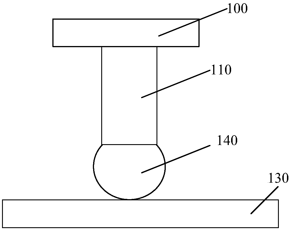
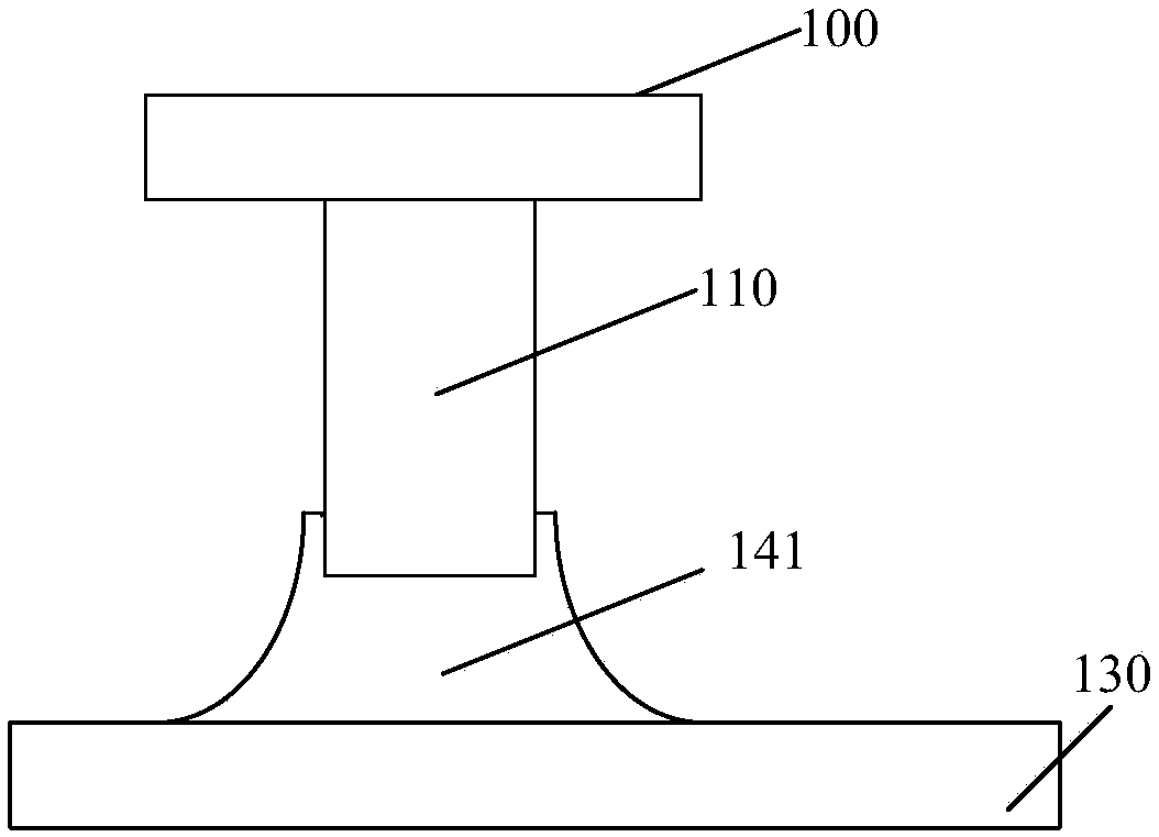
[0026] Figure 1 to Figure 2 is a schematic diagram of the structure of the flip-chip method.

[0027] refer to figure 1 , providing a semiconductor chip 100, a conductive connecting column 110 and a carrier plate 130, the conductive connecting column 110 has an opposite first surface and a second surface; the conductive connecting column 110 is fixed on the surface of the semiconductor chip 100, the first Facing the semiconductor chip 100; the solder ball 140 is fixedly arranged on the second surface of the conductive connection column 110; after that, the semiconductor chip 100, the conductive connection column 110 and the solder ball 140 are placed on the surface of the carrier board 130, and the solder ball 140 is connected to the surface of the carrier plate 130. The carrier board 130 is in surface contact.

[0028] refer to figure 2 A...


PUM


Abstract

The invention provides a packaging structure. The packaging structure comprises a semiconductor chip, and a conductive connection post which comprises opposite first and second sides. The first side of the conductive connection post is fixed with the surface of the semiconductor chip. The packaging structure further comprises a carrier board which is opposite to the semiconductor chip. The conductive connection post is located between the semiconductor chip and the carrier board, and the second side faces the carrier board. The packaging structure further comprises a solder layer located between the surface of the carrier board and the second side. The performance of the packaging structure is improved.

Description

technical field [0001] The invention relates to the packaging field, in particular to a packaging structure. Background technique [0002] The flip chip process is not only a chip interconnection technology, but also an ideal chip bonding technology. As early as more than 50 years ago, IBM (International Business Machines Corporation) has developed and used this technology. But until recent years, flip-chip has become a frequently used package formation in the field of high-end devices and high-density packaging. At present, the application range of flip-chip packaging technology is becoming wider and wider, and the packaging forms are becoming more diversified, and the requirements for flip-chips are also increasing. [0003] However, the performance of the package structure formed by the existing flip-chip method is poor. Contents of the invention [0004] The problem solved by the present invention is to provide a packaging structure to improve the performance of the...

Claims


Application Information

Patent Timeline
Patent Type & Authority Applications(China)
IPC IPC(8): H01L23/49
CPCH01L23/49H01L23/3128H01L23/3121H01L21/4853H01L23/49811H01L23/49541H01L23/4952H01L2224/81191H01L2224/81411H01L2224/81416H01L2224/16237H01L2224/10175H01L2224/81193H01L2224/13111H01L2224/13116H01L2224/81815H01L2224/13005H01L2224/16245H01L24/81H01L24/13H01L24/16H01L2224/13147H01L2924/3841H01L2924/014H01L2924/01047H01L2924/00014H01L2924/01029H01L2924/01082H01L2924/0105H01L2924/206H01L23/3114H01L24/33H01L24/17H01L21/56H01L23/49816H01L23/481H01L24/73
Inventor 石磊
Owner NANTONG FUJITSU MICROELECTRONICS
Why Eureka
Try Eureka