Flexible wiring circuit board, manufacturing method thereof, and imaging device
A wiring circuit substrate and manufacturing method technology, applied in printed circuit manufacturing, radiation control devices, printed circuits, etc., can solve problems such as noise and malfunction of electronic components, and achieve warpage suppression, good mountability, and excellent mountability. Effect
- Summary
- Abstract
- Description
- Claims
- Application Information
AI Technical Summary
Problems solved by technology
Method used
Image

Examples
no. 2 Embodiment approach >
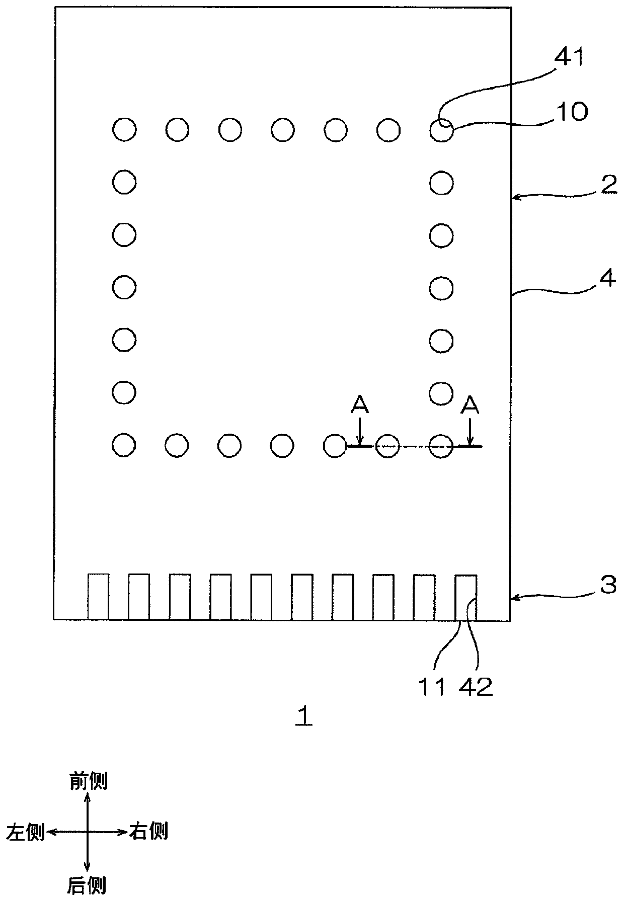
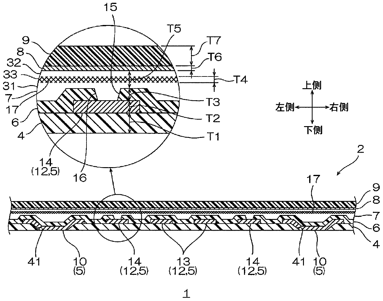
[0204] Reference Figure 9~Figure 10C The second embodiment of the mounting board 1 will be described. In addition, in the mounting board 1 of the second embodiment, the figure 2 The same components in the first embodiment shown are denoted by the same reference numerals, and the description thereof is omitted.
[0205] In contrast to the structure of the first embodiment, the mounting substrate 1 of the second embodiment further includes a second conductor pattern 50 and a fourth insulating layer between the first insulating cover layer 6 and the anisotropic conductive adhesive layer 7 The third cover insulating layer 51.
[0206] That is, the mounting substrate 1 of the second embodiment includes an insulating base layer 4, a conductive pattern (first conductive pattern) 5, a first insulating cover layer 6, a second conductive pattern 50, a third insulating cover layer 51, and anisotropic conductive The adhesive layer 7, the shielding layer 8, and the second insulating cover la...
no. 3 Embodiment approach >
[0235] Reference Picture 11 The third embodiment of the mounting board 1 will be described. In addition, in the mounting board 1 of the third embodiment, the figure 2 with Picture 9 The same members of the first embodiment and the second embodiment shown are denoted by the same reference numerals, and the description thereof is omitted.
[0236] Compared with the structure of the first embodiment, the mounting substrate 1 of the third embodiment further includes a second adhesive layer as a second adhesive layer between the first insulating cover layer 6 and the anisotropic conductive adhesive layer 7. The anisotropic conductive adhesive layer 60, the second insulating base layer 61, the second conductor pattern 50 and the third insulating cover layer 51.
[0237] That is, the mounting substrate 1 of the third embodiment includes an insulating base layer 4, a conductor pattern (first conductor pattern) 5, a first insulating cover layer 6, a second anisotropic conductive adhesive...
no. 3 Embodiment approach
[0248] The third embodiment also exhibits the same effects as those of the first and second embodiments.
[0249] In particular, in the third embodiment, compared with the first embodiment, the degree of freedom of wiring design can be increased.
[0250] In addition, the mounting substrate 1 of the third embodiment includes a second anisotropic conductive adhesive layer 60 between the first wiring 12 and the second wiring 52, and the second anisotropic conductive adhesive layer 60 contains reinforcement Cellulose layer 17. Therefore, the thermal expansion coefficient of the second anisotropic conductive adhesive layer 60 decreases. Therefore, the warpage of the imaging unit 27 can be further suppressed.
[0251] In addition, the modification of the first embodiment can be similarly applied to the third embodiment.
[0252] In addition, in the mounting substrate 1 of the above embodiment, the second adhesive layer is the second anisotropic conductive adhesive layer 60. However, for ...
PUM
| Property | Measurement | Unit |
|---|---|---|
| Thickness | aaaaa | aaaaa |
| Thickness | aaaaa | aaaaa |
| Thickness | aaaaa | aaaaa |
Abstract
Description
Claims
Application Information
 - Generate Ideas
- Intellectual Property
- Life Sciences
- Materials
- Tech Scout
- Unparalleled Data Quality
- Higher Quality Content
- 60% Fewer Hallucinations
Browse by: Latest US Patents, China's latest patents, Technical Efficacy Thesaurus, Application Domain, Technology Topic, Popular Technical Reports.
© 2025 PatSnap. All rights reserved.Legal|Privacy policy|Modern Slavery Act Transparency Statement|Sitemap|About US| Contact US: help@patsnap.com