
LED display unit board

A display unit, LED lamp bead technology, applied in static indicators, instruments, etc., can solve the problems of PCB cost increase, cost increase, device failure rate increase, etc., to facilitate PCB layout, reduce failure rate and coupling phenomenon, and reduce power consumption. The effect of consumption and heat

Inactive Publication Date: 2019-12-20
浙江德广信电子科技股份有限公司
View PDF14 Cites 0 Cited by
  • Summary
  • Abstract
  • Description
  • Claims
  • Application Information

AI Technical Summary

Problems solved by technology

[0008] 1. Too many display unit boards will lead to increased cost and poor splicing effect; too few unit boards will lead to high production and processing precision and increase maintenance costs
[0009] 2. The single package light source leads to poor protection, which increases the maintenance cost of production costs; the production cost and maintenance cost of COB package light source are too high, and the uniformity of light emission is difficult to solve perfectly
[0010] 3. The red LED light has a voltage of about 2v, and the green and blue lights have a voltage of about 3v. The existing scheme of 4-5v voltage power supply leads to an increase in power consumption of the entire screen, and the red, green, and blue common anode drive causes a voltage difference between the red lights, which is converted into heat and causes a temperature rise. High, resulting in regional color cast and lifetime
[0011] 4. The separation of the existing drive chip constant current drive and row mos tubes makes the small-pitch layout difficult, increases the cost of the PCB, and the separation of the chips makes the coupling serious, the failure rate of too many devices increases, and the maintenance cost increases

Method used


Image

  • LED display unit board
  • LED display unit board
  • LED display unit board

Examples


Embodiment Construction

[0053] In order to better explain the present invention and facilitate understanding, the present invention will be described in detail below through specific embodiments in conjunction with the accompanying drawings.

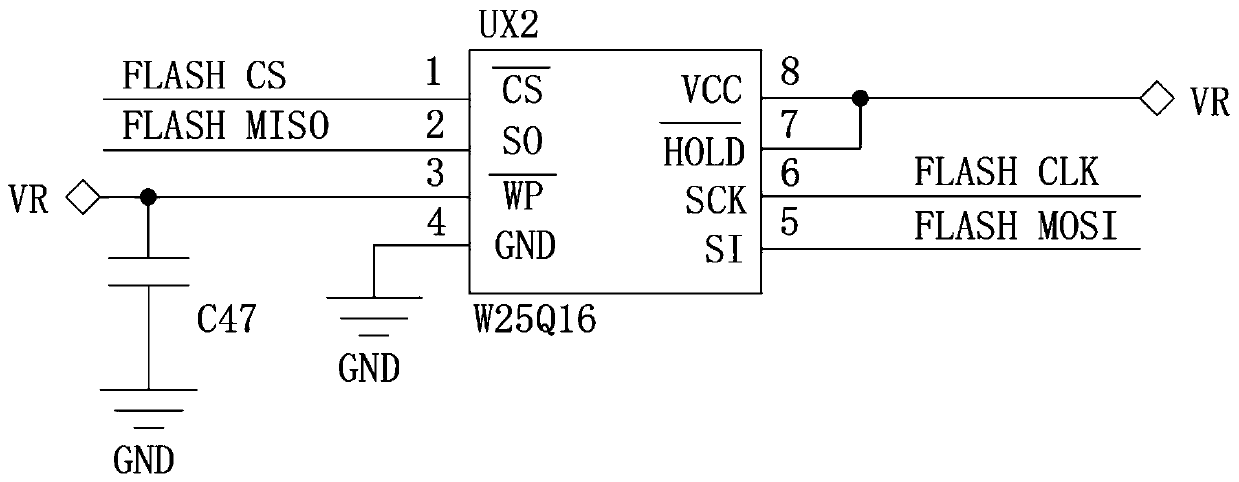
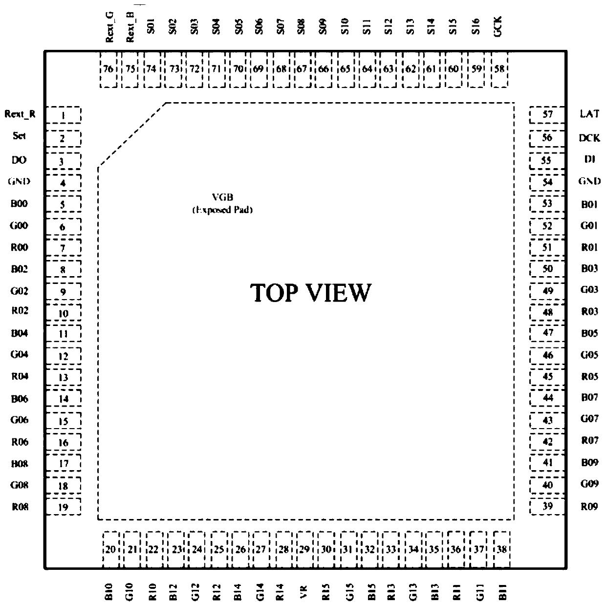
[0054] This embodiment discloses an LED display unit board, comprising: an HDI PCB board, a plurality of mini 4-in-1 full-color LED lamp beads surface-attached on the lamp surface of the HDI PCB board, and a plurality of row-column-in-one integrated chips.

[0055] The use of four-in-one surface-mounted lamp beads can solve the problem of small spacing and easy bumping without increasing production costs.

[0056] In detail, the multiple rank-in-one integrated chips described here are connected in series for communication. Before that, it should be explained that the HDI PCB in this embodiment is integrated with numerous circuits, and the circuits here are used to realize the connection of various components assembled on the HDI PCB.

[0057] The multiple row-...


PUM


Abstract

The invention relates to an LED display unit board. The LED display unit board comprises an HDI PCB, a plurality of mini four-in-one full-color LED lamp beads and a plurality of row-column integratedchips, wherein the mini four-in-one full-color LED lamp beads and the row-column integrated chips are attached to the lamp face of the HDI PCB. The plurality of row-column integrated integrated chipsare connected in series for communication; the plurality of row-column integrated chips are connected with a circuit on the HDI PCB; the plurality of mini four-in-one full-color LED lamp beads are connected with a circuit on the HDI PCB; a circuit on the HDI PCB can send video data control information to the plurality of row-column integrated chips; and the plurality of row-column integrated chipscan convert the received video data control information into a control signal, and control the work of the plurality of mini four-in-one full-color LED lamp beads by virtue of a circuit on the HDI PCB, so as to display the video information on the lamp surface in an image form. The display unit board provided by the invention greatly reduces power consumption and heat, and is energy-saving and environment-friendly.

Description

technical field [0001] The invention belongs to the technical field of LED display screens, in particular to an LED display unit board. Background technique [0002] The current industry LED display unit boards have a variety of small-pitch design schemes, mainly as follows: [0003] 1. Display unit board size: the existing schemes include 12, 8 and 2 boards. [0004] 2. Selection of Led light source: There are two existing solutions for Led light source: single lamp and COB. [0005] 3. LED drive mode: the current scheme basically adopts 4.2-5v voltage power supply, and the red, green and blue light-emitting chips are driven by common anode. [0006] 4. LED driver chip: The existing solution uses a constant current chip and a row mos tube to drive separately. [0007] Defects of prior art solutions [0008] 1. Too many display unit boards will lead to increased cost and poor splicing effect; too few unit boards will lead to high production and processing precision and i...

Claims


Application Information

Patent Timeline
Patent Type & Authority Applications(China)
IPC IPC(8): G09G3/32
CPCG09G3/32
Inventor 王明臣赵毅
Owner 浙江德广信电子科技股份有限公司
Learn More