Semiconductor structure and formation method thereof

A semiconductor and regional technology, applied in the direction of semiconductor devices, semiconductor/solid-state device manufacturing, electrical components, etc., can solve the problems of LDMOS withstand voltage performance to be improved, and achieve the effect of extending length, improving withstand voltage performance, and reducing voltage gradient

Active Publication Date: 2019-12-17
SEMICON MFG INT (SHANGHAI) CORP +1
View PDF5 Cites 5 Cited by
  • Summary
  • Abstract
  • Description
  • Claims
  • Application Information

AI Technical Summary

Problems solved by technology

[0005] However, after the introduction of fin field effect transistors in LDMOS, the withstand voltage performance of LDMOS still needs to be improved

Method used


Image

  • Semiconductor structure and formation method thereof
  • Semiconductor structure and formation method thereof
  • Semiconductor structure and formation method thereof

Examples


Embodiment Construction

[0016] It can be seen from the background art that after the fin field effect transistor is introduced into the LDMOS, the withstand voltage performance of the LDMOS needs to be improved. Combining with a semiconductor structure, the reason why its withstand voltage performance needs to be improved is analyzed.

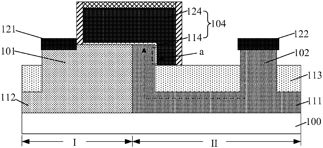
[0017] refer to figure 1 , shows a schematic structural view of a semiconductor structure.

[0018] The semiconductor structure includes: a substrate 100, a fin (not marked) protruding from the substrate 100, and the substrate 100 includes a first region I and a second region II adjacent to each other, located in the second region The fin at the junction of the first region I and the second region II is the first fin 101, the fin located in the second region II is the second fin 102; the well region 112, the fin located in the first region I part and the substrate 100; the drift region 111 is located in the fin part of the second region II and the substrate 100; the...


PUM


Abstract

The invention discloses a semiconductor structure and a formation method thereof. The method comprises the steps of providing a base, wherein the base comprises a substrate and a fin portion located on the substrate, the base comprising a first region and a second region which are adjacent to each other, the fin portion stretches across the first region and the second region along an extension direction, a well region is formed in the base of the first region, and a drift region is formed in the base of the second region; forming a gate oxide layer covering the top surface and the side wall surface of the fin portion; forming a gate layer on the gate oxide layer at the junction of the first region and the second region, wherein the gate layer stretches across the fin portion and covers part of the top and part of the side wall of the fin portion; forming a source region in the well region on one side of the gate layer, and forming a drain region in the drift region on the other side ofthe gate layer; sequentially etching the gate layer, the gate oxide layer and partial thickness of the base in the drift region in part of the second region on one side of the drain region after theformation of the source region and the drain region, and forming an isolation groove in the drift region; and forming an isolation layer in the isolation groove. According to the invention, the voltage withstanding performance of the LDMOS is facilitated to be improved.

Description

technical field [0001] The invention relates to the field of semiconductor manufacturing, in particular to a semiconductor structure and a forming method thereof. Background technique [0002] As semiconductor chips are used more and more widely, there are more and more factors that cause semiconductor chips to be damaged by static electricity. In existing chip designs, electrostatic discharge (ESD, Electrostatic Discharge) protection circuits are often used to reduce chip damage. The design and application of existing ESD protection circuits include: Gate Grounded NMOS (GGNMOS for short) protection circuit, Silicon Controlled Rectifier (SCR for short) protection circuit, lateral double diffusion field Effect transistor (Lateral Double Diffused MOSFET, LDMOS for short) protection circuit, bipolar junction transistor (Bipolar Junction Transistor, BJT for short) protection circuit, etc. Among them, LDMOS is widely used in ESD protection because it can withstand a higher brea...

Claims


Application Information

Patent Timeline
Patent Type & Authority Applications(China)
IPC IPC(8): H01L29/78H01L21/336
CPCH01L29/7816H01L29/785H01L29/66681H01L29/66795
Inventor 周飞
Owner SEMICON MFG INT (SHANGHAI) CORP
Why Eureka
Try Eureka