Three-dimensional packaging structure of MEMS infrared detector and manufacturing method of three-dimensional packaging structure

An infrared detector, three-dimensional packaging technology, applied in measurement devices, microstructure technology, microstructure devices, etc., can solve the problems of different absorption rates, picture distortion, large thermal stress, etc., to achieve good electrical performance, small thermal stress, The effect of low loss

Pending Publication Date: 2019-12-17
NANTONG UNIVERSITY
View PDF5 Cites 0 Cited by
  • Summary
  • Abstract
  • Description
  • Claims
  • Application Information

AI Technical Summary

Problems solved by technology

Common bonding methods such as Cu-Sn bonding and Au-Sn bonding are not only costly, but also prone to large thermal stress
[0004] In addition, the existing MEMS infrared detectors have different absorption rates for different frequencies of light, which may easily cause picture distortion under specific environmental requirements

Method used


Image

  • Three-dimensional packaging structure of MEMS infrared detector and manufacturing method of three-dimensional packaging structure
  • Three-dimensional packaging structure of MEMS infrared detector and manufacturing method of three-dimensional packaging structure
  • Three-dimensional packaging structure of MEMS infrared detector and manufacturing method of three-dimensional packaging structure

Examples


Embodiment Construction

[0037] The technical solutions in the embodiments of the invention will be clearly and completely described below in conjunction with the accompanying drawings in the embodiments of the invention. Obviously, the described embodiments are only some, not all, embodiments of the invention. Based on the embodiments of the present invention, all other embodiments obtained by persons of ordinary skill in the art without making creative efforts fall within the protection scope of the present invention.

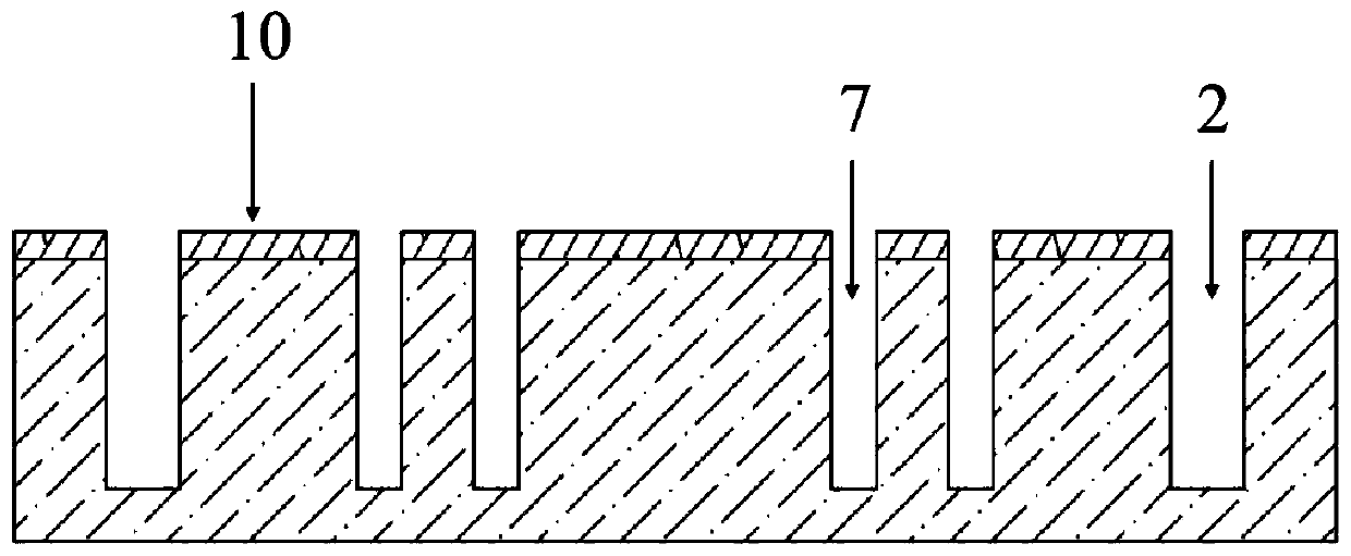
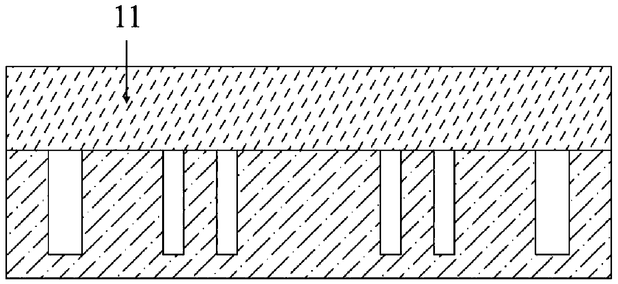
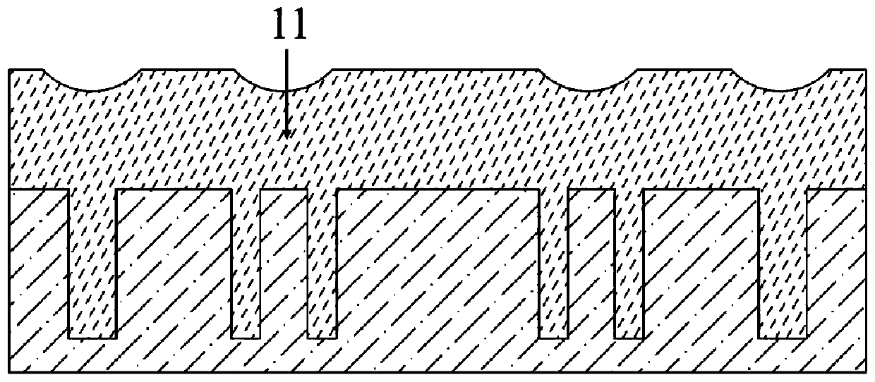
[0038] The application provides a MEMS infrared detector three-dimensional packaging structure, including a silicon substrate 1, the silicon substrate 1 is longitudinally provided with two vertical conductive regions, each vertical conductive region includes a vertical silicon lead 6 and a vertical silicon lead 6 peripheral The electrical isolation layer 8, the silicon substrate 1 is configured to accommodate the packaging chamber 5 of the MEMS infrared detector, the silicon substrate...


PUM


Abstract

The invention provides a three-dimensional packaging technology of an MEMS infrared detector, which is characterized in that a silicon wafer is provided with two vertical conductive area glass refluxgrooves and a vertical lead, and embedded borosilicate glass is used as an electric insulation layer of the lead and a substrate. A sub-wavelength structure array is arranged at the top of the packaging cover. According to the three-dimensional packaging structure provided by the invention, internal and external electrical interconnection is realized based on the low-resistance silicon vertical lead prepared by a glass reflow process, and the borosilicate glass and the low-resistance silicon have matched thermal expansion coefficients, so that the thermal stress is relatively low. The sub-wavelength structure array at the top of the packaging cover is used for enhancing the infrared transmission performance in a long-wave infrared region. A package chamber is prepared below the sub-wavelength structure array to accommodate the infrared detector. In addition, the invention further provides a manufacturing method of the packaging structure.

Description

technical field [0001] The invention belongs to the technical field of packaging, and in particular relates to a packaging structure of a MEMS infrared detector and a manufacturing method thereof. Background technique [0002] In recent years, microelectromechanical system (MEMS) infrared detectors, including thermopile, thermal radiation meter, pyroelectric detector and resonant detector, etc., have been widely used in military due to their small size, high resolution, low cost and CMOS compatible process. It has broad application prospects in civil and civil fields. For MEMS infrared detectors, relatively backward packaging technology has become one of the main bottlenecks restricting MEMS infrared detector products from entering the market. Packaging technology will directly affect the performance, cost and size of MEMS infrared detector products. [0003] Wafer-level three-dimensional packaging technology is conducive to the miniaturization of MEMS infrared detector pa...

Claims


Application Information

Patent Timeline
Patent Type & Authority Applications(China)
IPC IPC(8): B81B7/00B81B7/02B81C1/00G01J5/20G01J5/22
CPCB81B7/02B81B7/007B81B7/0009B81C1/00214B81C1/00301B81C1/00325B81B7/0045G01J5/20G01J5/22G01J2005/202B81B2203/0315B81B2201/0207B81C1/00317B81B2207/095G01J5/045
Inventor 赵继聪诸政葛明敏高波宋晨光孙玲孙海燕
Owner NANTONG UNIVERSITY
Why Eureka
Try Eureka