How to make a multilayer circuit board

A technology of multilayer circuit board and manufacturing method, which is applied in multilayer circuit manufacturing, printed circuit manufacturing, printed circuit, etc., and can solve problems such as poor analysis of outer layer circuits, increased accessories process, and etched circuits.

Active Publication Date: 2021-09-14
AVARY HLDG (SHENZHEN) CO LTD +1
View PDF10 Cites 0 Cited by
  • Summary
  • Abstract
  • Description
  • Claims
  • Application Information

AI Technical Summary

Problems solved by technology

[0003] However, the manufacturing method of this multilayer circuit board has the following disadvantages: 1. The combination of the outer layer and the inner layer is formed by pressing the single and double panels with pure glue, and the single panel and the pure glue need to be opened separately
If you make a multi-layer board with more than three layers, the assembly process will be multiplied
2. When making the outer circuit, when using dry film to protect the inner layer and analyze the outer circuit, it often occurs that the circuit at the inner layer is etched or the outer circuit is poorly resolved, which makes the reliability of the circuit board poor.

Method used


Image

  • How to make a multilayer circuit board
  • How to make a multilayer circuit board
  • How to make a multilayer circuit board

Examples


Embodiment Construction

[0028] In order to further illustrate the technical means and effects that the present invention takes to reach the intended purpose of the invention, the following in conjunction with the appended Figure 1-8 And the preferred implementation mode, the specific implementation mode, structure, features and effects of the method for manufacturing a multilayer circuit board provided by the present invention are described in detail as follows.

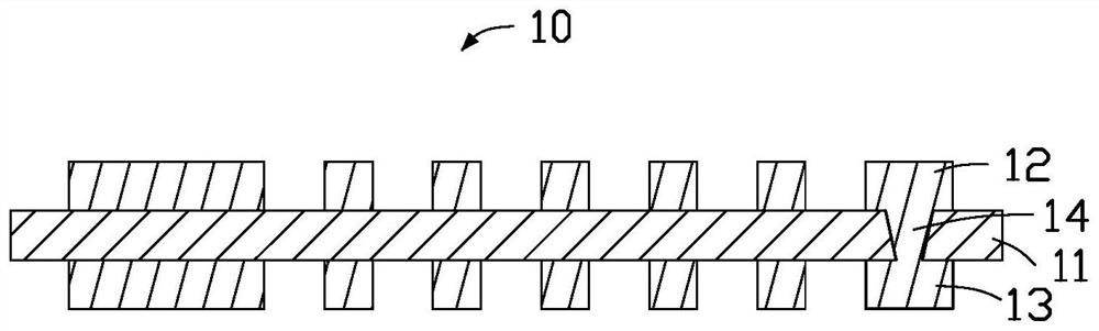
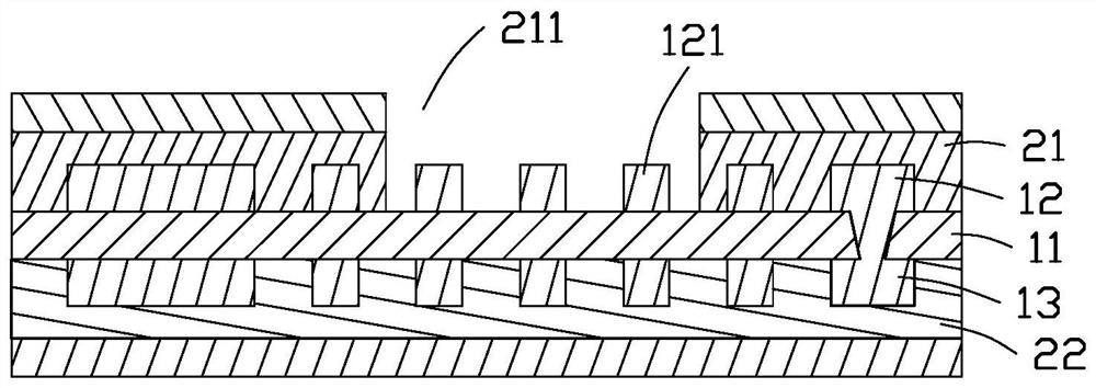
[0029] see Figure 1-8 , the present invention provides a method for manufacturing a multilayer circuit board 100, comprising the following steps:

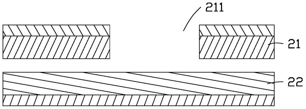
[0030] For a first step, see Figure 1-2 , providing an inner layer circuit substrate 10 , a first cover film 21 and a second cover film 22 .

[0031] Wherein, the inner circuit substrate 10 includes a base material layer 11 and a first conductive circuit layer 12 and a second conductive circuit layer 13 formed on opposite surfaces of the base material layer 11 .

[0032] Wherein, the subst...


PUM


Abstract

A method for manufacturing a multilayer circuit board, comprising the following steps: providing an inner circuit substrate, the inner circuit substrate at least including a base material layer and a first conductive circuit layer formed on a surface of the base material layer; The first conductive circuit layer includes a plurality of first conductive circuits; a first cover film is formed on the first conductive circuit layer, and the first cover film includes a first opening, and a part of the first conductive circuit from the first exposed in the opening; an outer line seed layer is formed on the first cover film, and an inner line protection layer is formed on the first conductive line exposed from the first opening, and the inner line protection layer The layer is non-copper metal or resist; forming a third conductive circuit layer on the outer circuit seed layer; and removing the outer circuit seed layer and the inner circuit protection layer. The manufacturing method of the multi-layer circuit board provided by the invention can reduce work flow and improve circuit reliability.

Description

technical field [0001] The invention relates to a printed circuit board technology, in particular to a method for manufacturing a multilayer circuit board. Background technique [0002] The multilayer circuit board includes an inner layer circuit substrate and an outer layer circuit. In the prior art, the manufacturing method of the outer layer circuit board is as follows: the outer layer single-sided board and the pure glue of the connection layer are respectively opened and then pressed with the inner layer circuit substrate, and then the outer layer circuit is manufactured through an image transfer process. Among them, it is necessary to use dry film or peelable adhesive to protect the inner circuit and resolve the outer circuit. [0003] However, the manufacturing method of this multilayer circuit board has the following disadvantages: 1. The combination of the outer layer and the inner layer is formed by pressing the single and double panels with pure glue, and the sin...

Claims


Application Information

Patent Timeline
Patent Type & Authority Patents(China)
IPC IPC(8): H05K3/46
CPCH05K3/4644H05K2203/1377
Inventor 杨梅戴俊
Owner AVARY HLDG (SHENZHEN) CO LTD
Why Eureka
Try Eureka