Blind buried hole printed circuit board and manufacturing method thereof

A technology of printed circuit boards and manufacturing methods, which is applied in the direction of printed circuit manufacturing, printed circuits, printed circuits, etc., can solve the problems of line width/spacing requirements, inability to make dense lines, and inability to guarantee reliability, so as to reduce plating Copper times, reduce the outer layer copper thickness, improve the effect of line density

Pending Publication Date: 2019-11-29
珠海杰赛科技有限公司 +1
View PDF0 Cites 2 Cited by
  • Summary
  • Abstract
  • Description
  • Claims
  • Application Information

AI Technical Summary

Problems solved by technology

The conductive connection between the layers of the existing blind buried via printed circuit board is to drill holes after lamination, and then metallize the holes to realize interlayer interconnection. Multiple times of pressing, each blind pressing, the board will age after multiple pressings, and even lead to failure during subsequent assembly and welding, and after multiple pressings and metallization of holes, the surface copper thickness will also decrease. It will thicken accordingly, making it difficult to etch the circuit later, and it is impossible to make a circuit-dense board, which runs counter to the high-density function of blind buried holes.
In the prior art, the number of pressing times of blind buried holes is generally controlled below 3 times (inclusive), and there are requirements for line width / spacing. If a printed circuit board with 4 blind holes on the same layer needs to be pressed 4 times, reliability cannot be guaranteed. sex

Method used


Image

  • Blind buried hole printed circuit board and manufacturing method thereof
  • Blind buried hole printed circuit board and manufacturing method thereof
  • Blind buried hole printed circuit board and manufacturing method thereof

Examples


Embodiment Construction

[0028] In order to describe the technical content, achieved goals and effects of the present invention in detail, the following descriptions will be made in conjunction with the embodiments and accompanying drawings.

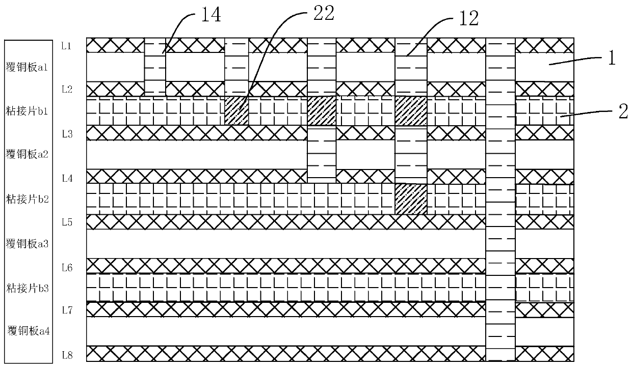
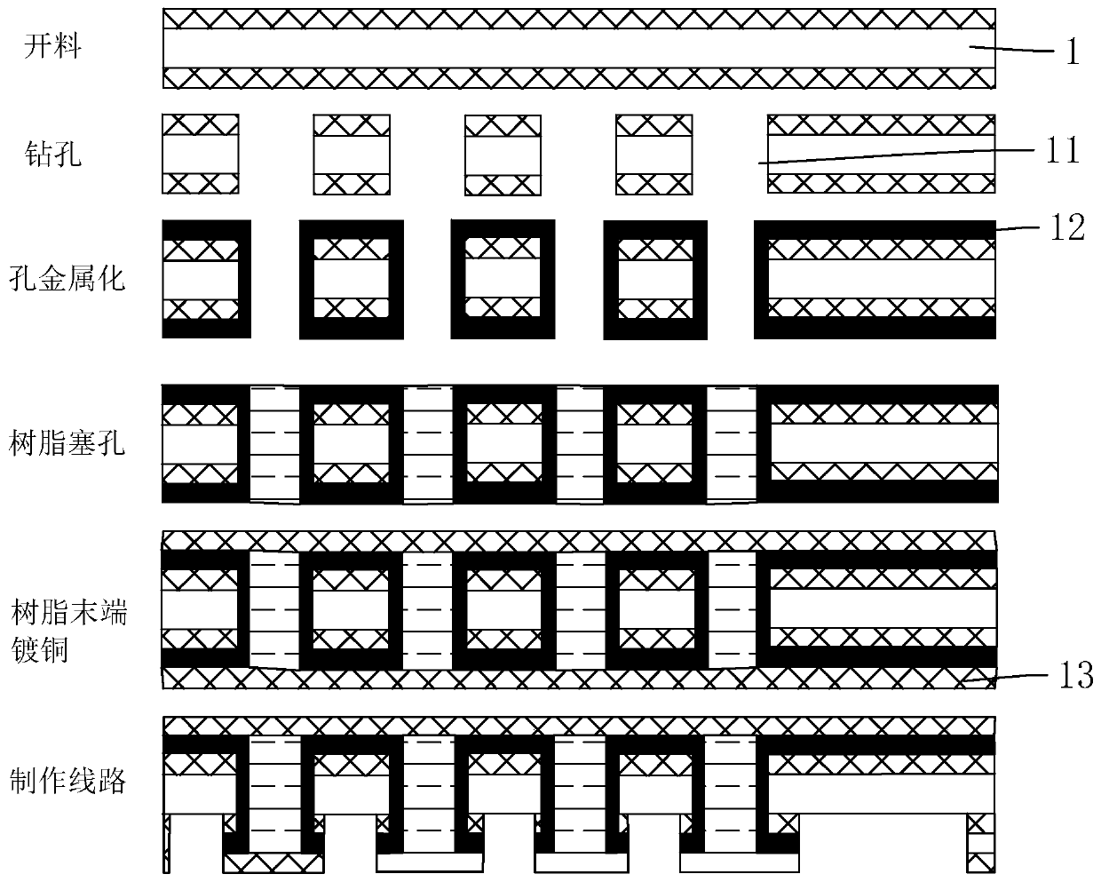
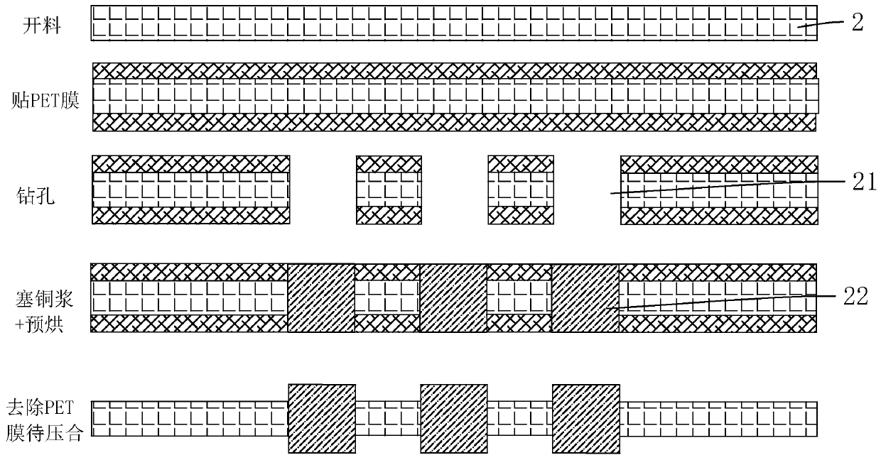
[0029] Such as figure 1 Shown is a printed circuit board with blind buried vias of the present invention, including: four-layer copper clad laminates 1 stacked in sequence and three-layer adhesive sheets 2 arranged between two adjacent layers of copper clad laminates, and the copper clad laminates are provided with The first opening 11, the adhesive sheet is provided with a second opening 21 corresponding to the first opening 11, the first opening 11 is filled with a resin column 14, the inner wall of the first opening 11 and the resin column 14 are arranged There is a first metal layer 12, the end of the resin column 14 is covered with a second metal layer 13, the first metal layer 12 is connected to the second metal layer 13, the second opening 21 is filled wi...


PUM


Abstract

The invention discloses a blind buried hole printed circuit board, and the circuit board comprises multiple layers of copper-clad plates, and bonding sheets arranged between two adjacent layers of copper-clad plates; resin columns are disposed in the copper-clad plates, and second metal layers are disposed at the tail ends of the resin columns, wherein a first metal layer is connected with the second metal layers; copper paste is disposed in the bonding sheets, wherein the copper paste is connected with the second metal layers. The invention further comprises a manufacturing method of the blind buried hole printed circuit board. Holes are formed in the positions, corresponding to the blind buried holes, of the bonding sheets, and the copper paste is plugged into the holes; the copper pasteand a metal film are sintered together in the pressing process of the bonding sheets and the copper-clad plates, thereby achieving the interlayer interconnection; a PET film is attached to the bonding sheets before the bonding sheets are plugged into the holes through the copper paste for protection. According to the technical scheme, the lamination frequency can be reduced, the production efficiency can be improved, a printed circuit board with a blind buried hole structure can be realized for many times, the outermost layer copper plating frequency can be reduced, the outer layer copper thickness can be reduced, a smaller line width / spacing can be manufactured, and the circuit density of the circuit board can be improved.

Description

technical field [0001] The invention relates to the field of printed circuit board processing and manufacturing, in particular to a printed circuit board with blind buried holes and a manufacturing method thereof. Background technique [0002] With the development of electronic products towards miniaturization, high density, and high precision, correspondingly higher requirements are put forward for printed circuit boards, and printed circuit boards with blind and buried vias appear for the purpose of dense wiring. The conductive connection between the layers of the existing blind buried via printed circuit board is to drill holes after lamination, and then metallize the holes to realize interlayer interconnection. Multiple times of pressing, each blind pressing, the board will age after multiple pressings, and even lead to failure during subsequent assembly and welding, and after multiple pressings and metallization of holes, the surface copper thickness will also decrease....

Claims


Application Information

Patent Timeline
Patent Type & Authority Applications(China)
IPC IPC(8): H05K1/11H05K3/42H05K3/46
CPCH05K1/115H05K3/421H05K3/429H05K3/4611H05K2201/09509H05K2201/09563
Inventor 刘国汉杨杰
Owner 珠海杰赛科技有限公司
Why Eureka
Try Eureka