Layout correction method

A technology of layout and graphics, applied in the field of layout correction, can solve the problems of actual graphics distortion, disconnection, uneven distribution of light energy, etc., and achieve the effect of ensuring no distortion

Pending Publication Date: 2019-11-29
SHANGHAI HUALI MICROELECTRONICS CORP
View PDF11 Cites 0 Cited by
  • Summary
  • Abstract
  • Description
  • Claims
  • Application Information

AI Technical Summary

Problems solved by technology

[0004] On this basis, when exposing the semiconductor substrate based on the pattern on the mask plate, since the width of the first pattern of each target pattern is small, and the width of the second pattern is relatively large, the light in The connection between the second pattern and the first pattern is very prone to the problem of uneven distribution of light energy caused by the optical proximity effect (Optical Proximity Effect, OPE), resulting in the fact that the first pattern and the first pattern in the actual pattern finally formed on the substrate Disconnection occurs at the junction of the second pattern; at the same time, because the first pattern A1 of the target pattern A is closer to the second pattern B2 of another target pattern B, it will result in the actual pattern finally formed on the semiconductor substrate. The first pattern A1 and the second pattern B2 are glued together, so that the actual pattern finally formed on the semiconductor substrate is severely distorted

Method used


Image

  • Layout correction method
  • Layout correction method
  • Layout correction method

Examples


Embodiment Construction

[0037] The layout correction method proposed by the present invention will be further described in detail below in conjunction with the accompanying drawings and specific embodiments. Advantages and features of the present invention will be apparent from the following description and claims. It should be noted that the drawings are all in a very simplified form and use inaccurate scales, and are only used to facilitate and clearly assist the purpose of illustrating the embodiments of the present invention.

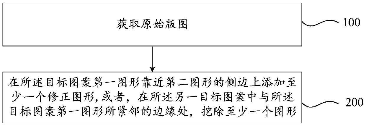
[0038] figure 2 A schematic flowchart of a layout correction method provided by an embodiment of the present invention, as shown in Figure 2, the method may include:

[0039] Step 100, obtaining the original layout.

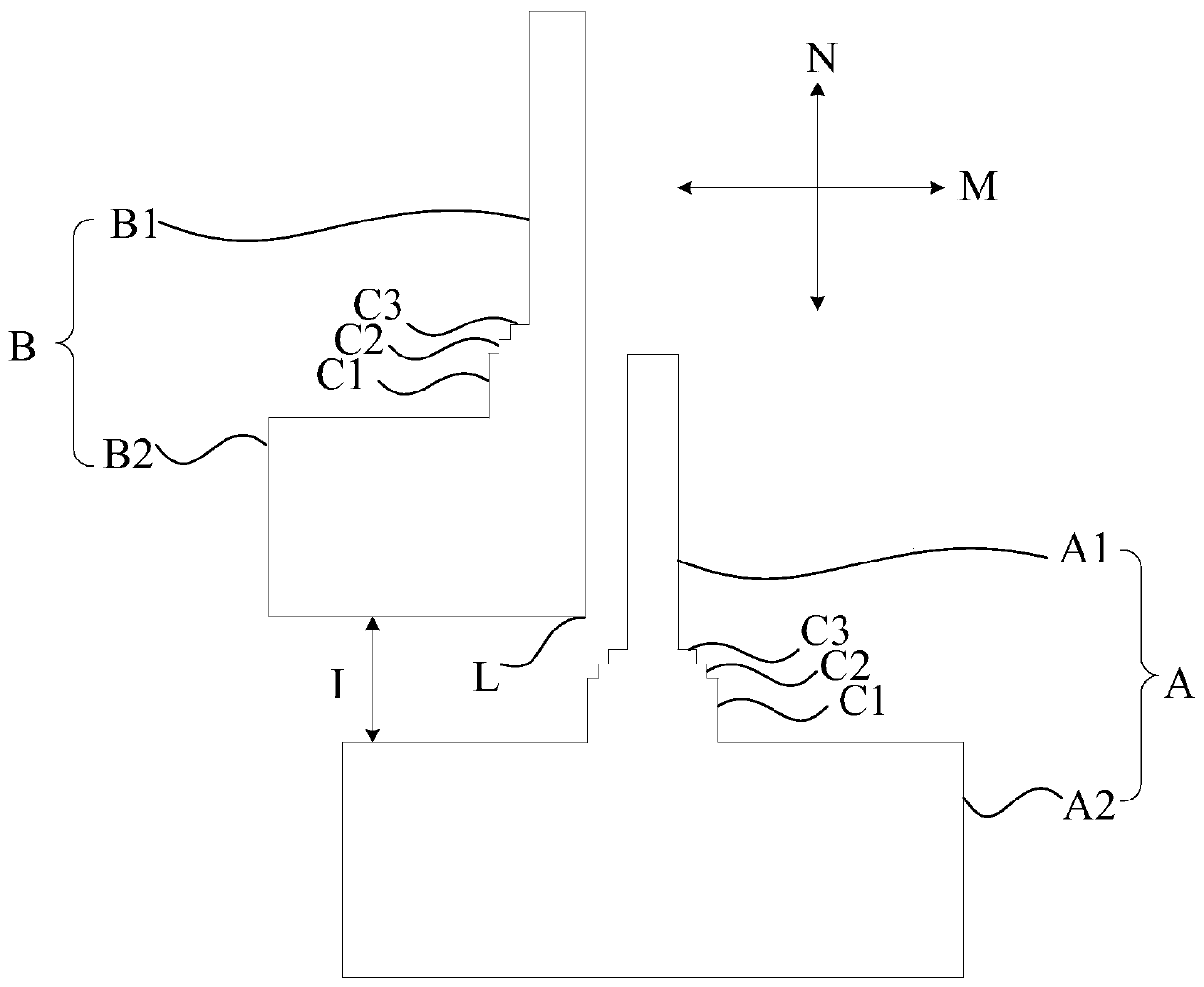
[0040]The original layout may include at least two target patterns, the target pattern includes a first graphic and a second graphic, the first graphic may be a bar structure, and the first graphic and the second graphic are connected One or both sides of...


PUM


Abstract

The invention provides a layout correction method, which comprises steps: an original layout is obtained, wherein the original layout comprises at least two target patterns, the target pattern comprises a first pattern and a second pattern, the first pattern is of a strip-shaped structure, the first pattern is connected with the second pattern, the second pattern of the other target pattern is arranged on one side or two sides of the first pattern of the target pattern, and the second pattern of the target pattern and the second pattern of the other target pattern are arranged at an interval;and at least one correction pattern is added to the side edge, close to the second pattern, of the first pattern of the target pattern, or, at least one pattern is dug out at the edge, close to the first pattern of the target pattern, of the other target pattern. After the layout correction method provided by the invention is adopted to complete correction, the manufactured mask plate can be additionally provided with process windows for exposure, and process defects such as line breakage or adhesion and the like are effectively avoided, so that an actual pattern finally formed on the substrate is ensured not to be distorted.

Description

technical field [0001] The invention relates to the technical field of semiconductor manufacturing, in particular to a layout correction method. Background technique [0002] In the manufacturing process of semiconductor devices, the semiconductor substrate is usually exposed based on the mask, so that the pattern on the mask is transferred to the semiconductor substrate, so that the semiconductor substrate can be subsequently developed, etched and other steps. [0003] However, in the related art, there are generally multiple target patterns on the mask, and each target pattern specifically includes two graphics, for example, the reference figure 1 The target pattern A in includes a first graphic A1 and a second graphic A2, the first graphic A1 is a long bar, and the first graphic A1 is connected to the second graphic A2, and the second graphic A2 There is a large difference in width from the width of the first graphic A1. At the same time, another target pattern B is adj...

Claims


Application Information

Patent Timeline
IPC IPC(8): G03F1/72G03F1/36
CPCG03F1/72G03F1/36Y02P90/30
Inventor 刘洋刘建忠顾晓敏
Owner SHANGHAI HUALI MICROELECTRONICS CORP
Why Eureka
Try Eureka