Three-dimensional memory and preparation method thereof

A memory and three-dimensional technology, applied in the semiconductor field, can solve problems such as poor contact, current path disconnection, and high threshold voltage of three-dimensional memory

Active Publication Date: 2019-11-22
YANGTZE MEMORY TECH CO LTD
View PDF4 Cites 4 Cited by
  • Summary
  • Abstract
  • Description
  • Claims
  • Application Information

AI Technical Summary

Problems solved by technology

However, as the market’s requirements for storage density continue to increase, the number of three-dimensional memory stack layers continues to increase, and the aspect ratio of the CH becomes larger. The etching process of the memory stack at the bottom of the CH is facing greater challenges.
If the memory stack layer at the bottom of the CH is not removed clean

Method used


Image

  • Three-dimensional memory and preparation method thereof
  • Three-dimensional memory and preparation method thereof
  • Three-dimensional memory and preparation method thereof

Examples


preparation example Construction

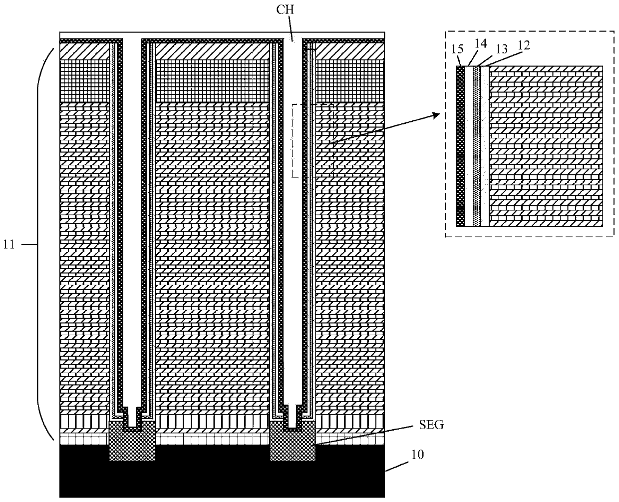
[0054] Based on this, an embodiment of the present invention provides a method for manufacturing a three-dimensional memory; for details, please refer to image 3 . As shown, the method includes the following steps:

[0055] Step 101, providing a stacked structure, the stacked structure including a number of alternately stacked dielectric layers and sacrificial layers, and a channel hole CH penetrating through the stacked structure;

[0056] Step 102, forming a pre-storage layer on the sidewall of the CH;

[0057] Step 103, removing the sacrificial layer to expose the pre-storage layer;

[0058] Step 104 , oxidize the pre-storage layer at the position where the sacrificial layer is removed, so as to form a relatively outer barrier layer and a relatively inner storage layer along the CH radial direction.


PUM


Abstract

The embodiment of the invention discloses a three-dimensional memory and a preparation method thereof, and the method comprises the following steps: providing a laminated structure which comprises a plurality of dielectric layers and sacrificial layers, wherein the dielectric layers and the sacrificial layers are alternately laminated, and a channel through hole CH passing through the laminated structure; forming a pre-storage layer on the side wall of the CH; removing the sacrificial layers, and exposing the pre-storage layer; and oxidizing the pre-storage layer at the position where the sacrificial layers are removed so as to form a barrier layer which is relatively close to the outer side and a storage layer which is relatively close to the inner side along the radial direction of the CH.

Description

technical field [0001] The invention relates to the technical field of semiconductors, in particular to a three-dimensional memory and a preparation method thereof. Background technique [0002] Memory is a memory device used to save information in modern information technology. With the continuous improvement of the demand for integration and data storage density of various electronic devices, it is increasingly difficult for ordinary two-dimensional memory devices to meet the requirements. In this case, three-dimensional (3D) memory emerges as the times require. [0003] In a three-dimensional memory, the memory stack functions to control the storage of memory charges, and is the key structure for the device to complete the storage function. At present, the commonly used structure of the memory stack is barrier layer-storage layer-tunneling layer; the above layers are formed by sequential deposition in the channel hole (Channel Hole, CH); after the deposition of the above...

Claims


Application Information

Patent Timeline
IPC IPC(8): H01L27/1157H01L27/11582
CPCH10B43/35H10B43/27
Inventor 王启光
Owner YANGTZE MEMORY TECH CO LTD
Why Eureka
Try Eureka