Cuprous oxide/cuprous thiocyanate heterojunction photoelectric film and preparation method thereof

A cuprous thiocyanate, photoelectric thin film technology, applied in photovoltaic power generation, circuits, electrical components and other directions, can solve the problem of high recombination rate of photogenerated carriers, achieve low cost, improve photoelectrochemical performance, and achieve obvious modification effect. Effect

Active Publication Date: 2019-11-19
CHINA JILIANG UNIV
View PDF2 Cites 4 Cited by
  • Summary
  • Abstract
  • Description
  • Claims
  • Application Information

AI Technical Summary

Problems solved by technology

In the present invention, the CuSCN photoelectric thin film prepared by electrochemical deposition is soaked in alkali solution for a certain period of time to promote the in-situ reaction of CuSCN to generate Cu 2 O, realized the in situ construction of Cu 2 O / CuSCN heterojunction photoelectric thin film solves the problem of high recombination rate of photogenerated carriers in CuSCN photoelectric thin film to a large extent, and greatly improves the photoelectrochemical performance of copper thiocyanate photoelectric thin film

Method used


Image

  • Cuprous oxide/cuprous thiocyanate heterojunction photoelectric film and preparation method thereof
  • Cuprous oxide/cuprous thiocyanate heterojunction photoelectric film and preparation method thereof
  • Cuprous oxide/cuprous thiocyanate heterojunction photoelectric film and preparation method thereof

Examples


Embodiment 1

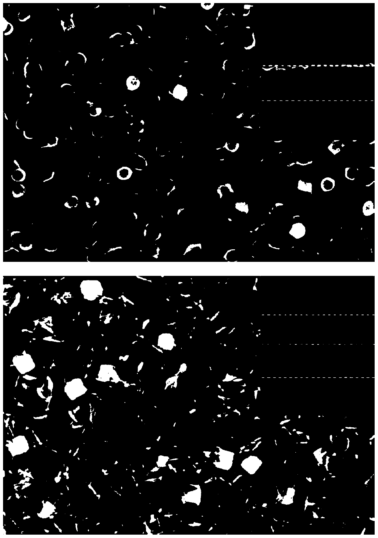
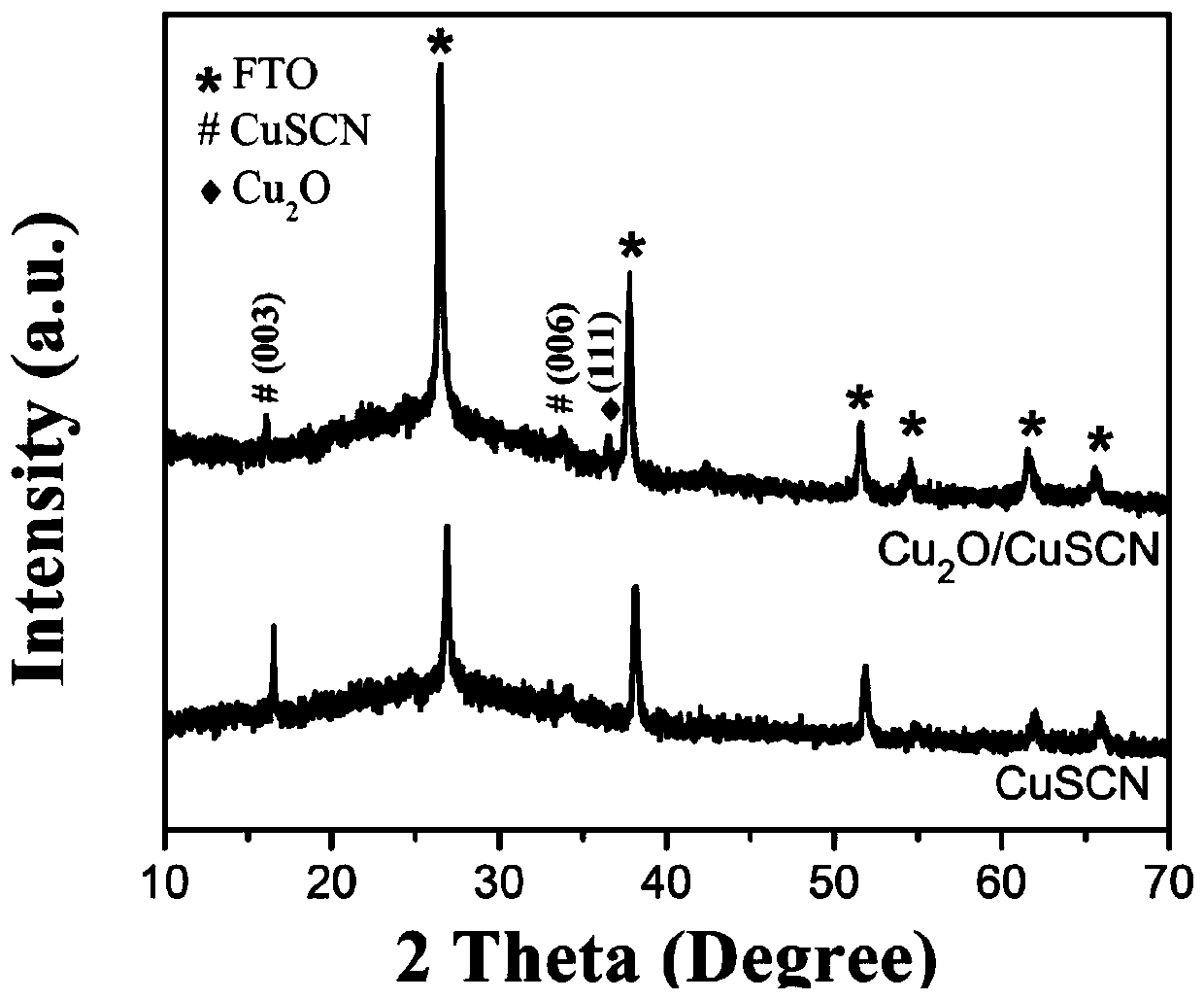
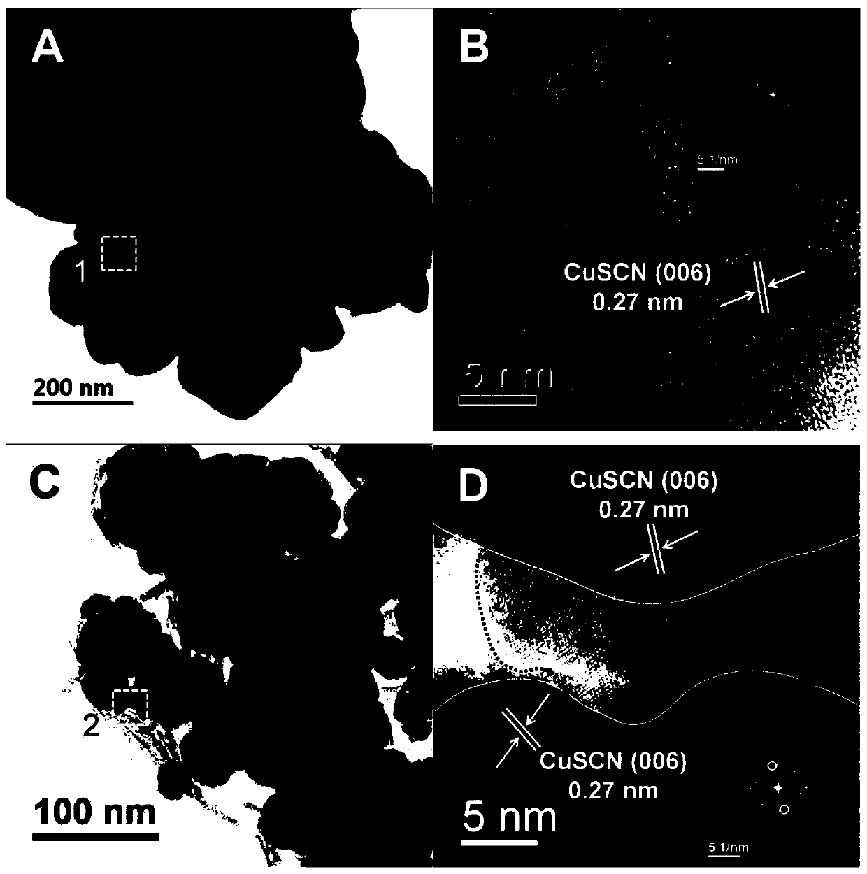
[0018] (1) Dissolve 2.4 mmol of copper sulfate pentahydrate, 2.4 mmol of ethylenediaminetetraacetic acid (EDTA) and 0.6 mmol of potassium thiocyanate (KSCN) in 200 mL of deionized water, stir well and prepare the precursor solution; the precursor solution prepared above was transferred to a three-electrode system electrochemical reaction tank equipped with a platinum wire counter electrode (platinum wire), a calomel reference electrode and a cleaned FTO conductive glass, at a deposition potential of -0.4 V, deposited charge is 80 mC / cm 2 Electrochemical deposition was carried out under the conditions; the FTO conductive glass after the electrochemical deposition was rinsed twice with deionized water, 60 o After drying in a vacuum oven, CuSCN photoelectric thin films were prepared.

[0019] (2) Soak the CuSCN film prepared above in 0.05 mol / L NaOH solution for 90 s, take it out and rinse it twice with deionized water to obtain the CuSCN film grown in situ 2 O / CuSCN heterojunc...

Embodiment 2

[0021] (1) The preparation process of the CuSCN photoelectric thin film is the same as in Example 1.

[0022] (2) On the premise of obtaining the above-mentioned CuSCN photoelectric thin film, soak the CuSCN thin film in 0.05 mol / L NaOH solution for 30 s, take it out and rinse it twice with deionized water, and then the CuSCN film grown in situ can be obtained. 2 O / CuSCN heterojunction photoelectric thin film.

Embodiment 3

[0024] (1) The preparation process of the CuSCN photoelectric thin film is the same as in Example 1.

[0025] (2) On the premise of obtaining the above-mentioned CuSCN photoelectric thin film, soak the CuSCN thin film in 0.05 mol / L NaOH solution for 180 s, take it out and rinse it twice with deionized water to obtain the in-situ grown Cu 2 O / CuSCN heterojunction photoelectric thin film.


PUM


Abstract

The invention belongs to the technical field of semiconductor photoelectricity, and particularly relates to a cuprous oxide/cuprous thiocyanate (Cu2O/CuSCN) heterojunction photoelectric film and a preparation method thereof. The invention provides a Cu2O/CuSCN heterojunction photoelectric thin film and a preparation method thereof. The method comprises the following steps that; a CuSCN photoelectric thin film prepared through electrochemical deposition is subjected to alkali liquor soaking treatment for a certain period of time to prompt the CuSCN to react in situ to generate Cu2O so that theCu2O/CuSCN heterojunction photoelectric thin film is constructed in situ. The problems of relatively low photo-generated carrier mobility, relatively high recombination rate and the like of the CuSCNphotoelectric thin film are solved to a relatively large extent, and the photoelectrochemical performance of the CuSCN photoelectric thin film is greatly improved. The Cu2O/CuSCN heterojunction photoelectric thin film and the preparation method thereof provided by the invention have the advantages that the modification means is simple, the heterojunction structure is easy to regulate and control,the modification effect is obvious, the cost is low and the like.

Description

technical field [0001] The invention belongs to the technical field of semiconductor optoelectronics, and in particular relates to a cuprous oxide / cuprous thiocyanate heterojunction photoelectric thin film and a preparation method thereof. Background technique [0002] In recent years, p-type semiconductor thin films have received great attention and been widely used as hole transport layers or photocathode materials in the field of photoelectrochemistry (such as photocatalytic water splitting, photocatalysis, solar cells, photovoltaic devices, sensors, etc.) . For the practical application of optoelectronic devices, the ideal p-type semiconductor thin film requires: excellent hole carrier mobility, suitable energy band structure, good structural stability, wide electrochemical reaction window, easy synthesis, Features such as low cost. At present, p-type semiconductor materials mainly include three types: small organic molecules (such as: spiro-OMeTAD), organic polymers (...

Claims


Application Information

Patent Timeline
Patent Type & Authority Applications(China)
IPC IPC(8): H01L31/032H01L31/0352H01L31/0392H01L31/072H01L31/18
CPCH01L31/032H01L31/035272H01L31/0392H01L31/072H01L31/18Y02E10/50Y02P70/50
Inventor 李灵惠陈达秦来顺黄岳祥梁俊辉
Owner CHINA JILIANG UNIV
Why Eureka
Try Eureka