


Quick Research
Generate reliable direction feasibility study reports for your R&D in just a few steps.

Technical Q&A
Discover and master advanced knowledge NOW. Basics, ideas, possibilities, all at once.

Find Solutions
As an expert in R&D theories, this can generate solutions to your technical problems instantly.

Evaluate Feasibility
Analyze your overall solution with one click, know your potential R&D risks in advance.

Monitor Landscape
Get weekly tech updates, stay abreast of the latest tech innovations and key insights.
Touch sensing film and processing method, device and application thereof
A technology of touch sensing and processing methods, which is applied in the directions of instruments, computing, and electrical digital data processing, etc., which can solve the problems of complex process, thick touch panel, and high manufacturing cost, and achieve simple process, low cost, and precise and controllable processing Effect
- Summary
- Abstract
- Description
- Claims
- Application Information
AI Technical Summary
Problems solved by technology
Method used
Image


Examples
Embodiment 1-7
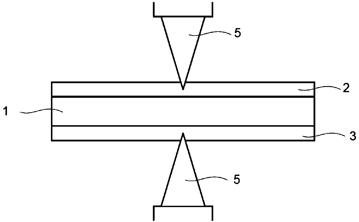
[0058] This embodiment provides a touch sensing film and a processing method thereof, wherein the touch sensing film includes a first conductive layer 2, a second conductive layer 3 and a substrate layer 1, and the substrate layer 1 is arranged on the first conductive layer 2 and the second conductive layer 3.
[0059] The touch sensing film is etched by a laser etching method, wherein the wavelength range of the laser is set according to the material of the substrate layer; the energy density of the laser is greater than the etching threshold of the conductive layer, and the After the material layer is reduced to less than the etching threshold of the conductive layer.
[0060] Such as figure 1 As shown, on the side of the first conductive layer 2, the first conductive layer 2 is etched by laser 5. After the laser 5 passes through the substrate layer 1, the energy density decreases, and there is no damage to the second conductive layer 3; at the same time , on the side of t...
Embodiment 8
[0079] This embodiment provides a processing device for a touch sensitive film, such as Figure 14 As shown, the apparatus includes a laser etching assembly 18 to etch the conductive layer using a laser.
[0080] The above-mentioned laser etching assembly 18 includes a first laser emitter 5a and a second laser emitter 5b, and the first laser emitter 5a and the second laser emitter 5b are arranged on both sides of the track of the touch sensitive film for processing, so as to realize Simultaneous processing of the conductive layers on both sides of the touch sensitive film improves production efficiency.
[0081] The processing device also includes three pairs of driving rollers 13: a first driving roller 13a, a second driving roller 13b and a third driving roller 13c. The driving rollers 13 are used to drive the touch sensitive film to run to the laser etching assembly 18 for etching.
[0082] The processing device also includes an unwinding wheel 11 and a winding wheel 12, w...
PUM
| Property | Measurement | Unit |
|---|---|---|
| wavelength | aaaaa | aaaaa |
| wavelength | aaaaa | aaaaa |
| wavelength | aaaaa | aaaaa |
Abstract
Description
Claims
Application Information
 - R&D Engineer
- R&D Manager
- IP Professional
- Industry Leading Data Capabilities
- Powerful AI technology
- Patent DNA Extraction
Browse by: Latest US Patents, China's latest patents, Technical Efficacy Thesaurus, Application Domain, Technology Topic, Popular Technical Reports.
© 2024 PatSnap. All rights reserved.Legal|Privacy policy|Modern Slavery Act Transparency Statement|Sitemap|About US| Contact US: help@patsnap.com