Transparent electrode and electronic device
A transparent electrode and conductive layer technology, which is applied in the direction of electric solid devices, electrical components, semiconductor devices, etc., can solve the problems of atomic ratio distribution deviation and stability over time, and achieve sufficient conductivity and light transmittance. Excellent temporal stability and excellent uniformity of light emission
- Summary
- Abstract
- Description
- Claims
- Application Information
AI Technical Summary
Problems solved by technology
Method used
Image

Examples
example 1
[0174] [Configuration of Organic EL Elements Constituting Example 1]
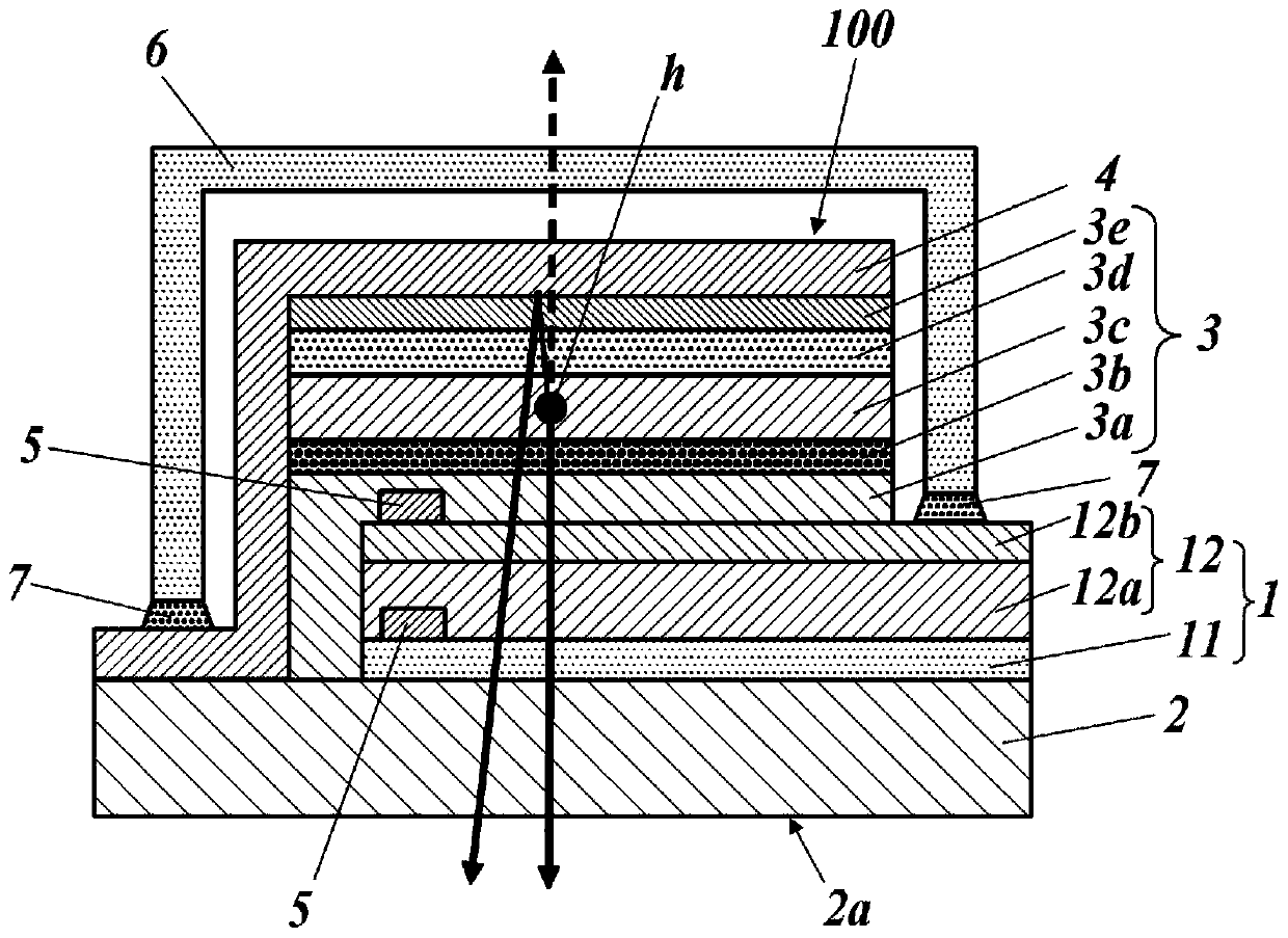
[0175] figure 2 is a schematic cross-sectional view of an organic EL element constituting Example 1.
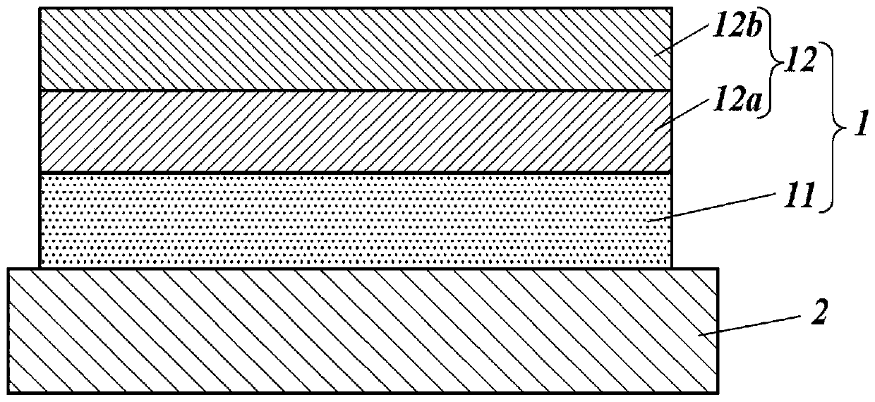
[0176] The organic EL element of this example is a so-called bottom emission type, that is, has a transparent substrate, and takes out light from the transparent substrate side. Specifically, as figure 2 As shown, the transparent electrode (1), the light-emitting functional layer (3) and the counter electrode (4) are sequentially stacked on the transparent substrate (2).
[0177] In this organic EL element (100), the transparent electrode (1) of the present invention described above is used as a transparent electrode. Therefore, the organic EL element (100) has a structure capable of extracting generated light (hereinafter, referred to as emitted light (h)) at least from the transparent substrate (2) side.
[0178] In addition, the layer structure of the organic EL element (100) is not limited to the...
example 2
[0289] [Configuration of organic EL element constituting Example 2]
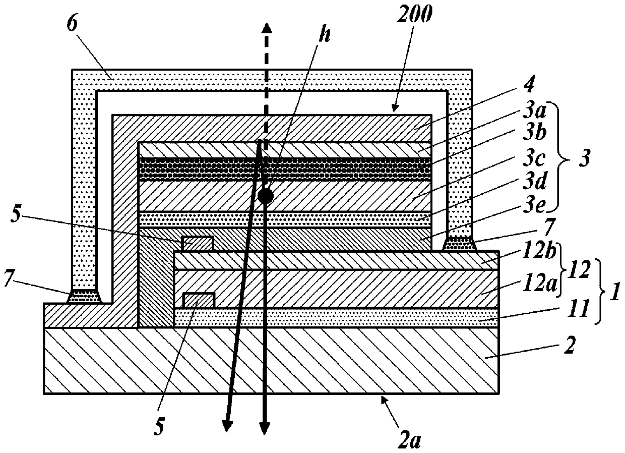
[0290] image 3 is a schematic cross-sectional view of an organic EL element constituting Example 2.
[0291] The organic EL element (200) of this example is the same as the configuration example 1, which is a bottom emission type, and is different from the above configuration example 1 in that the transparent electrode (1) is used as a cathode (the counter electrode (4) is an anode). Hereinafter, repeated detailed description of the same constituent elements as those constituting the organic EL element (100) of Example 1 will be omitted, and the characteristic configuration of the organic EL element (200) constituting Example 2 will be described.
[0292] Such as image 3 As shown, the organic EL element (200) is arranged on the transparent substrate (2), and figure 2 The structure example 1 shown is the same, and the above-mentioned transparent electrode (1) of the present invention is used as the tran...
example 3
[0304] [Configuration of organic EL element constituting Example 3]
[0305] Figure 4 is a schematic cross-sectional view showing a configuration example 3 of an organic EL element using the transparent electrode (1A) of the present invention as an example of the electronic device of the present invention.
[0306] Figure 4 The organic EL element (300) of the shown structural example 3 is a so-called top emission type, that is, the counter electrode (4A) is arranged on the substrate (2A) side, and the light-emitting functional layer (3), transparent electrode (1A) is formed on the surface. ) are stacked in the order of ), which is different from Configuration Example 1. Hereinafter, the characteristic configuration of the organic EL element ( 300 ) constituting Example 3 will be described without repeating detailed description of the same constituent elements as those in Configuration Example 1. FIG.
[0307] Figure 4 The organic EL element (300) shown is arranged on a ...
PUM
| Property | Measurement | Unit |
|---|---|---|
| Thickness | aaaaa | aaaaa |
| Thickness | aaaaa | aaaaa |
| Thickness | aaaaa | aaaaa |
Abstract
Description
Claims
Application Information
 - R&D
- Intellectual Property
- Life Sciences
- Materials
- Tech Scout
- Unparalleled Data Quality
- Higher Quality Content
- 60% Fewer Hallucinations
Browse by: Latest US Patents, China's latest patents, Technical Efficacy Thesaurus, Application Domain, Technology Topic, Popular Technical Reports.
© 2025 PatSnap. All rights reserved.Legal|Privacy policy|Modern Slavery Act Transparency Statement|Sitemap|About US| Contact US: help@patsnap.com