Optical chip substrate-based micro-spectral measurement device and method

An optical chip and spectrum measurement technology, applied in the field of microscopic spectrum analysis, can solve the problems of low analysis efficiency and slow collection speed, and achieve the effect of expanding the application range, simple structure and high integration

Active Publication Date: 2019-11-01
NANJING UNIV OF SCI & TECH
View PDF4 Cites 7 Cited by
  • Summary
  • Abstract
  • Description
  • Claims
  • Application Information

AI Technical Summary

Problems solved by technology

[0004] The purpose of the present invention is to provide a microspectral measurement device and method based on an optical chip substrate to solve the technical problems of slow collection speed and low analysis efficiency in traditional spectrum measurement

Method used


Image

  • Optical chip substrate-based micro-spectral measurement device and method
  • Optical chip substrate-based micro-spectral measurement device and method
  • Optical chip substrate-based micro-spectral measurement device and method

Examples


specific Embodiment 1

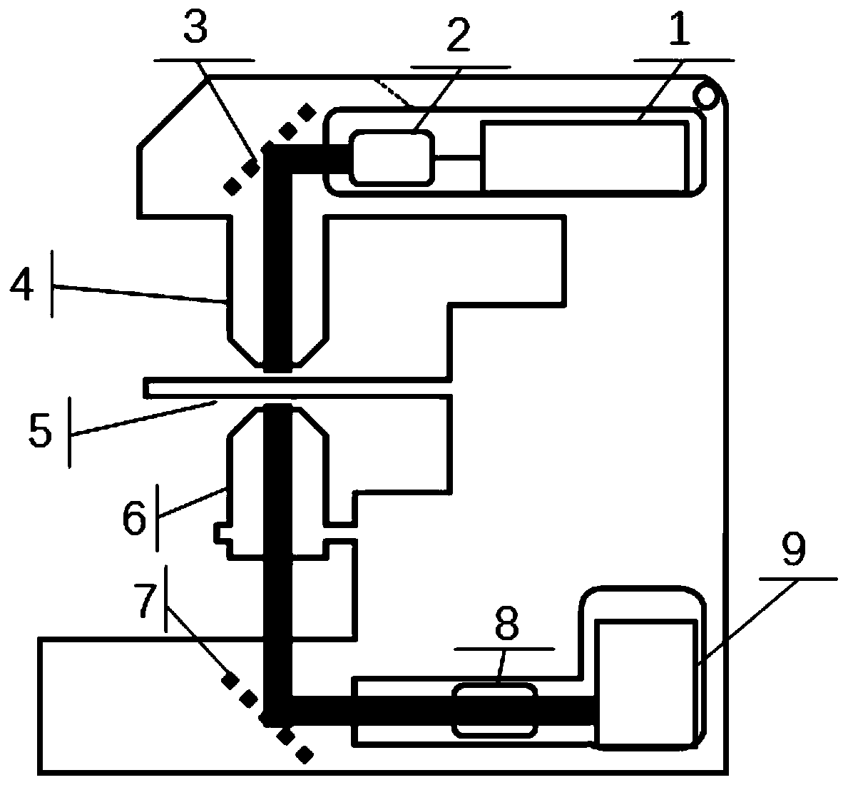
[0052] A microscopic spectrum measurement device based on an optical chip substrate includes an illumination laser light source 1, a beam expander lens 2, a near-end laser reflector 3, a focusing microscopic objective 4, a wide-spectrum coupling object-loading optical chip 5, and a collecting microscopic objective 6 , a dichroic mirror 7, an imaging lens 8 and an image sensor 9, wherein the wavelength of the illumination laser light source 1 is 532nm, which can excite carboxylic acid fluorescent molecules in the analyte. The wide-spectrum coupling object-loading optical chip 5 is composed of a polymer layer, a metal layer, a defect layer and a photonic crystal layer, wherein the polymer layer is PMMA with a thickness of 5nm; the metal layer material is silver with a thickness of 30nm; the defect layer is silicon dioxide, The thickness is 165nm; the photonic crystal layer is deposited alternately by silicon dioxide and silicon nitride, the thicknesses are respectively 125nm and ...


PUM

PropertyMeasurementUnit
thicknessaaaaaaaaaa
thicknessaaaaaaaaaa
thicknessaaaaaaaaaa

Abstract

The invention discloses an optical chip substrate-based micro-spectral measurement device and method. The device comprises an illumination laser source, a beam expansion lens, a near-end laser mirror,a focusing micro-objective, a wide spectral coupled carrier optical chip, a collection microscope, a dichroscope, an imaging lens and a CCD image sensor. The method comprises the following steps of preparing the wide spectral coupled carrier optical chip with a chromatic dispersion function; carrying out beam expansion on the laser emitted by the illumination laser source and reflecting the laserto a to-be-measured object on the chip through the near-end laser mirror and the focusing micro-objective; and constraining the signals sent by to-be-measured molecules on the surface of the wide spectral coupled carrier optical chip and enabling the signals to outgo downwards at a plurality of angles, and imaging the signals on the image sensor by the imaging lens after the signals are receivedby the micro-objective and reflected by the dichroscope so as to calculate a spectral signal of the to-be-measured object. The device and method is capable of solving the technical problem that the traditional spectral measurement is low in collection speed and low in analysis efficiency.

Description

technical field [0001] The invention relates to the technical field of microspectral analysis, in particular to a microspectral measurement device and method based on an optical chip substrate. Background technique [0002] Integrated chip technology based on surface light field regulation has achieved a series of breakthroughs in the fields of semiconductors, micromachining, and metamaterials, and has gradually moved from front-end research to practical applications. The research combined with its directional transmission characteristics has also made breakthroughs in the field of microscopic imaging such as high-contrast imaging and dark-field imaging. Using the confinement effect of the surface waveguide, it can well realize the observation of the sample morphology at different depths, but it cannot effectively reflect the composition and quantitative analysis of the sample. Because of this, the imaging technology widely used in photochemistry and biomedicine is often un...

Claims


Application Information

Patent Timeline
Patent Type & Authority Applications(China)
IPC IPC(8): G01N21/64G01N21/65G01N21/25
CPCG01N21/6458G01N21/65G01N21/255
Inventor 陈漪恺陈芙莲张璐丁彬轩沈中华
Owner NANJING UNIV OF SCI & TECH
Why Eureka
Try Eureka