Shell assembly, preparation method thereof and electronic device
A technology of housing components and areas, applied in branch equipment, telephone communication, electrical components, etc., can solve the problems of single housing style and cannot meet actual needs, and achieve the effect of rich styles
- Summary
- Abstract
- Description
- Claims
- Application Information
AI Technical Summary
Problems solved by technology
Method used
Image
Examples
preparation example Construction
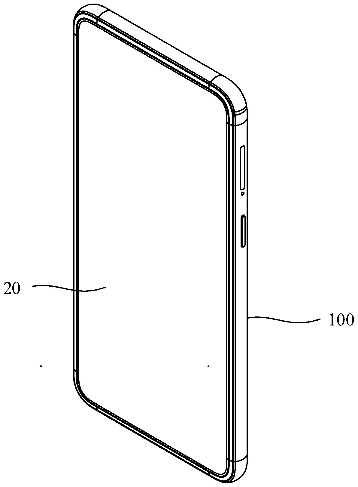
[0121] Please also see again Figure 1-9 , in addition, a method for preparing the shell assembly 100 of the first embodiment is also provided, including the following steps: S110-S130:
[0122] S110 , providing a transparent substrate 110 having a decorative surface 111 .
[0123] It should be noted that, the structure of the transparent substrate 110 can be referred to above, and will not be repeated here.
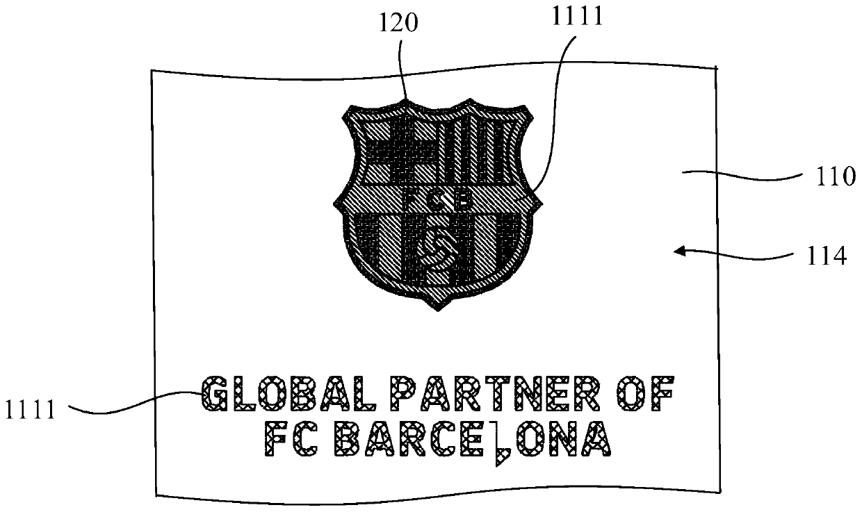
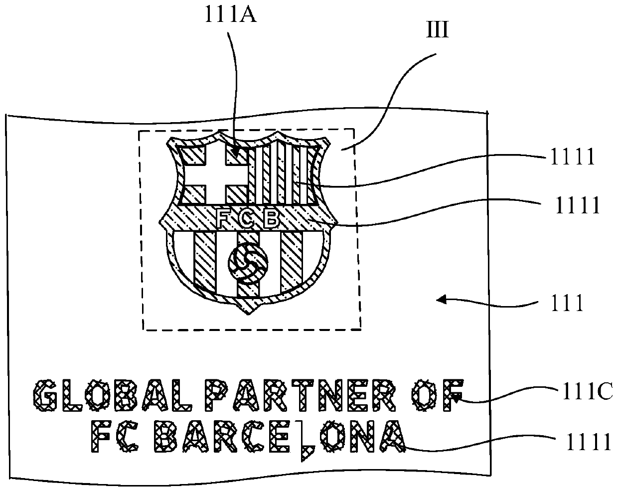
[0124] S120 , forming a plurality of spaced rough regions 1111 on the decoration surface 111 .
[0125] In one embodiment, the step of forming a plurality of spaced rough regions 1111 on the decorative surface 111 includes S121-S123:
[0126] Please also refer to Figures 14 to 15 , S121. Preset an ink area 1112 and a plurality of spaced areas to be decorated 1114 on the decoration surface 111, and the ink area 1112 is arranged around each area to be decorated 1114.
[0127] In one embodiment, the ink area 1112 is arranged around each to-be-decorated area 1114 .
[...
Embodiment 1
[0277] The structure of the shell assembly of the present embodiment is as Figure 1-9 As shown, the fabrication process of the shell assembly is as follows:
[0278] (1) Carry out the first CNC processing, hot bending treatment, second CNC processing and 3D polishing treatment on the transparent substrate in sequence. The thickness of the transparent substrate is 0.5 mm.
[0279] (2) Presetting an ink area and a plurality of spaced areas to be decorated on the decoration surface. The first ink is screen printed on the ink area for the first time, cured to obtain a cured part, the first ink is screen printed on the cured part for the second time, cured to obtain a first ink part, and the first ink part has multiple The first notch of the interval. The thickness of each printing is 5 μm. The first ink includes ink material and boiling water. The ink material is acid-resistant ink. The mass ratio of ink material to boiling oil and water is 98:3. During the first printing ...
Embodiment 2
[0292] The structure of the shell assembly of the present embodiment is as Figure 1-9 , the preparation process of the shell assembly is as follows:
[0293] (1) Carry out the first CNC processing, hot bending treatment, second CNC processing and 3D polishing treatment on the transparent substrate in sequence. The thickness of the transparent substrate is 0.7 mm.
[0294] (2) Presetting an ink area and a plurality of spaced areas to be decorated on the decoration surface. The first ink is screen printed on the ink area for the first time, cured to obtain a cured part, the first ink is screen printed on the cured part for the second time, cured to obtain a first ink part, and the first ink part has multiple The first notch of the interval. The thickness of each print is 8 μm. The first ink includes ink material and boiling water. The ink material is acid-resistant ink. The mass ratio of ink material to boiling oil and water is 102:7. During the first printing process, t...
PUM
 Abstract
Description
Claims
Application Information
 - R&D
- Intellectual Property
- Life Sciences
- Materials
- Tech Scout
- Unparalleled Data Quality
- Higher Quality Content
- 60% Fewer Hallucinations
Browse by: Latest US Patents, China's latest patents, Technical Efficacy Thesaurus, Application Domain, Technology Topic, Popular Technical Reports.
© 2025 PatSnap. All rights reserved.Legal|Privacy policy|Modern Slavery Act Transparency Statement|Sitemap|About US| Contact US: help@patsnap.com


