a ch-based 3 no 3 pbi 3 and al 2 o 3 Mos capacitive photosensitive device of material and preparation method thereof

A technology of photosensitive devices and capacitors, applied in semiconductor/solid-state device manufacturing, electric solid-state devices, electrical components, etc., can solve the development trend of low power consumption in the semiconductor industry, unfavorable miniaturization design of MOS devices, and dark state of MOS devices Large current and other problems, to achieve the effect of miniaturization design, excellent electrical characteristics, and reduce gate leakage current

Active Publication Date: 2021-03-23
XIDIAN UNIV
View PDF7 Cites 0 Cited by
  • Summary
  • Abstract
  • Description
  • Claims
  • Application Information

AI Technical Summary

Problems solved by technology

And with SiO 2 In MOS devices where insulating materials are used as gate dielectric materials, SiO 2 The thickness of the insulating material is usually hundreds of nanometers, resulting in a thicker overall thickness of the device, which is not conducive to the miniaturization design of MOS devices; moreover, SiO 2 The dark state current of MOS devices with insulating materials as the gate dielectric material is usually large, and the response speed of the device is slow, which does not conform to the development trend of low power consumption in the semiconductor industry

Method used


Image

  • a ch-based  <sub>3</sub> no  <sub>3</sub> pbi  <sub>3</sub> and al  <sub>2</sub> o  <sub>3</sub> Mos capacitive photosensitive device of material and preparation method thereof
  • a ch-based  <sub>3</sub> no  <sub>3</sub> pbi  <sub>3</sub> and al  <sub>2</sub> o  <sub>3</sub> Mos capacitive photosensitive device of material and preparation method thereof
  • a ch-based  <sub>3</sub> no  <sub>3</sub> pbi  <sub>3</sub> and al  <sub>2</sub> o  <sub>3</sub> Mos capacitive photosensitive device of material and preparation method thereof

Examples


Embodiment 1

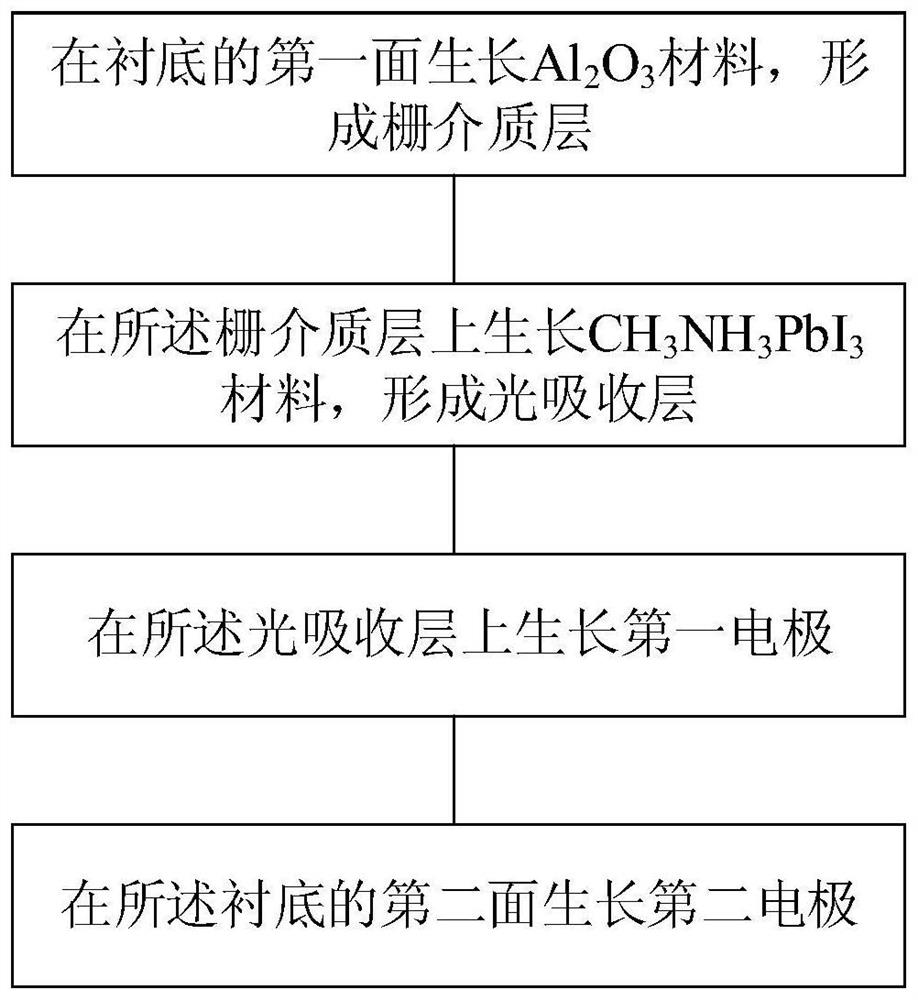
[0046] See figure 1 , figure 1 A CH-based 3 NH 3 PB 3 and Al 2 o 3 A schematic flow chart of the preparation method of the MOS capacitive photosensitive device of the material, including steps:

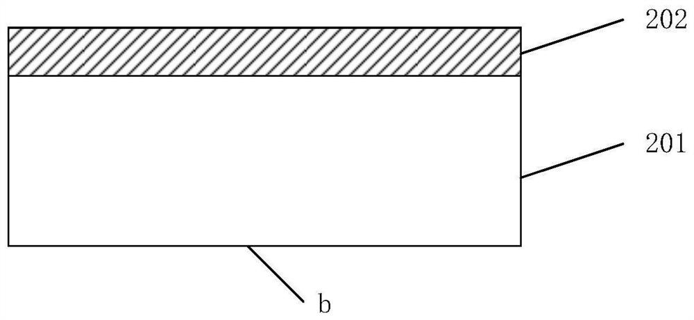
[0047] Al grows on the first side of the substrate 2 o 3 material to form a gate dielectric layer;

[0048] grow CH on the gate dielectric layer 3 NH 3 PB 3 material, forming the light absorbing layer;

[0049] growing a first electrode on the light absorbing layer;

[0050] A second electrode is grown on the second side of the substrate.

[0051] Specifically, see Figure 2a-Figure 2e , Figure 2a-Figure 2e A CH-based 3 NH 3 PB 3 and Al 2 o 3 The schematic diagram of the preparation method of the MOS capacitive photosensitive device of material, concrete steps are as follows:

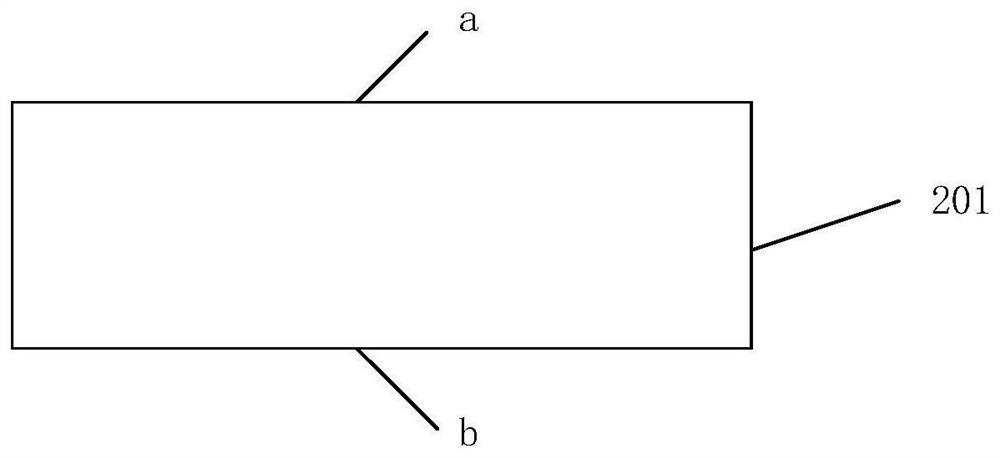
[0052] S1, select the substrate 201; please refer to Figure 2a .

[0053] Specifically, the material of the substrate 201 is Si. Select a bulk silicon material; the bulk silicon materi...

Embodiment 2

[0081] See Figure 4 with Figure 5 , Figure 4 A CH-based 3 NH 3 PB 3 and Al 2 o 3 Schematic diagram of the structure of the MOS capacitive photosensitive device of the material, Figure 5 for Figure 4 Provided based on CH 3 NH 3 PB 3 and Al 2 o 3 Top view of the MOS capacitive photosensitive device of the material.

[0082] The MOS capacitive photosensitive device includes: a second electrode 205 , a substrate 201 , a gate dielectric layer 202 , a light absorption layer 203 and a first electrode 204 .

[0083] Wherein, the material of the second electrode 205 is Al, and the thickness is 150 nm.

[0084] The substrate 201 is located on the second electrode 205 . The material of the substrate 205 is Si, the crystal orientation of the Si material is , the size is 4 inches, the thickness is 400 μm, the resistivity is 0.0015Ωcm, and the doping type is n-type

[0085] The gate dielectric layer 202 is located on the substrate 201 . The material of the gate dielect...


PUM

PropertyMeasurementUnit
thicknessaaaaaaaaaa
thicknessaaaaaaaaaa
thicknessaaaaaaaaaa

Abstract

The present invention relates to a CH-based 3 NH 3 PB 3 and Al 2 o 3 MOS capacitive photosensitive device of the material and its preparation method. Wherein, the preparation method includes the steps of: growing Al on the first surface of the substrate 2 o 3 material to form a gate dielectric layer; growing CH on the gate dielectric layer 3 NH 3 PB 3 materials to form a light absorbing layer; growing a first electrode on the light absorbing layer; growing a second electrode on the second surface of the substrate. The embodiment of the present invention MOS capacitive photosensitive device adopts Al 2 o 3 material as the gate dielectric layer, Al 2 o 3 The material is a high-K gate dielectric material. The high-K gate dielectric material makes the device almost non-conductive under dark state conditions, so that the current between the first electrode and the second electrode in the dark state is extremely small, and the gate leakage current is greatly reduced. , reduces the power consumption of the device, improves the photosensitive characteristics of the device, is conducive to reducing the characteristic size of the MOS device, and realizes the miniaturization design of the MOS device.

Description

technical field [0001] The invention belongs to the technical field of integrated circuits, in particular to a CH-based 3 NH 3 PB 3 and Al 2 o 3 MOS capacitive photosensitive device of the material and its preparation method. Background technique [0002] In recent years, due to the excellent photoelectric properties of organic-inorganic composite perovskite materials, such as strong light absorption ability, low electron-hole pair binding energy, long carrier diffusion length, and economic advantages such as simple preparation process and low preparation cost, In the field of solar cells by more and more research. From 2009 when Miyasaka et al. first applied perovskite as a light absorber in solar cells, in just a few years to 2019, the cell conversion efficiency has increased from 3.8% to 23.7%. [0003] So far, photodetectors based on organic-inorganic composite perovskite materials mainly have three structures: photoconductive structure, photodiode structure and ph...

Claims


Application Information

Patent Timeline
Patent Type & Authority Patents(China)
IPC IPC(8): H01L51/42H01L51/46H01L51/48
CPCH10K85/30H10K30/354H10K30/65Y02E10/549
Inventor 贾仁需刘晶煌李欢庞体强汪钰成杜永琪
Owner XIDIAN UNIV
Why Eureka
Try Eureka