Eureka AIR delivers breakthrough ideas for toughest innovation challenges, trusted by R&D personnel around the world.

Method for in situ production of majorana material superconductor hybrid networks and hybrid structure produced using the method

A hybrid structure, structuring technology, applied in the manufacture/processing of superconductor devices, superconductor components, nanotechnology for information processing, etc., can solve problems such as damage, very sensitive quantum state, state change, etc., to achieve good quality and performance effects

Pending Publication Date: 2019-09-27
KERNFORSCHUNGSANLAGE JUELICH GMBH
View PDF9 Cites 3 Cited by
  • Summary
  • Abstract
  • Description
  • Claims
  • Application Information

AI Technical Summary

Problems solved by technology

The main problem with a universal quantum computer is that the very sensitive and short-lived quantum state is unstable and the mere readout of this state can lead to a state change
Removal of subregions of the superconducting layer also disadvantageously always leads to changes or damage to the underlying material surface

Method used


Image

  • Method for in situ production of majorana material superconductor hybrid networks and hybrid structure produced using the method
  • Method for in situ production of majorana material superconductor hybrid networks and hybrid structure produced using the method
  • Method for in situ production of majorana material superconductor hybrid networks and hybrid structure produced using the method

Examples


Embodiment Construction

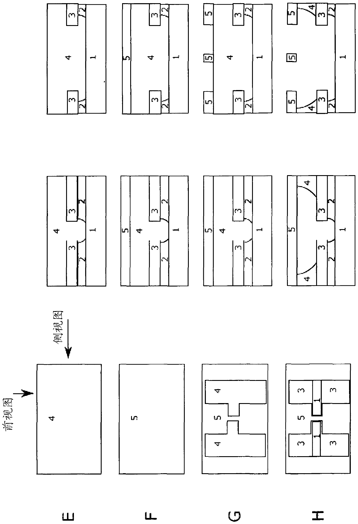
[0128] In the examples, preferred embodiments of the method according to the invention for producing Josephson contacts using structured Majorana materials and superconducting metals are described first. The definition of a Josephson contact should not be construed restrictively, but is also used as the smallest unit of a topological qubit for the explanation of the following embodiments. The letters of the process steps used to make the respective topological Josephson contacts here correspond to those in Figures 1 to 6 of those.

[0129] The method according to the invention comprises a plurality of functional layers, wherein in the following examples specific materials are mentioned for the application, which should not be construed as limiting. The method is divided into a total of three partial methods: preparation of the substrate for the structured deposition of the topological material (process step (I) "Selective Area"); application of the superconducting metal for t...


PUM

PropertyMeasurementUnit
Thicknessaaaaaaaaaa
Thicknessaaaaaaaaaa
Lengthaaaaaaaaaa

Abstract

The invention relates to a method for producing a Majorana material superconductor hybrid structure. The superconductive material is applied onto the Majorana material using a shadow mask, wherein a first mask (2, 3) for a structured application of the Majorana material (6) and an additional mask (shadow mask) (4, 5) for the structured growth of the superconductive material (7) are first generated on a substrate (1), the masks being aligned relative to each other, and the Majorana material and the superconductive layers are applied without interruption in an inert atmosphere, preferably in a vacuum and particularly preferably in an ultrahigh vacuum. The produced hybrid structure comprises at least one structured Majorana material, at least one superconductive material arranged thereon, and a passivation layer. The structured Majorana material has a wire-type design with a length between 0.1 and 100 [mu]m, a width between 10 and 200 nm, and a layer thickness between 12 and 260 nm, preferably between 15 and 50 nm. The boundary surface between the structured Majorana material and at least one superconductive material arranged thereon is advantageously free of contamination. The surface of the structured Majorana material is completely covered either by a preferably superconductive material or by a passivation layer.

Description

technical field [0001] The present invention relates to a method for producing a device that enables superconducting and Majorana materials in different geometries and dimensions down to a precision of a few nanometers in an inert atmosphere and preferably in an ultrahigh vacuum deposited in alignment with respect to each other and sealed with a passivation protection layer. Complex networks composed of the mentioned materials can be fabricated with this device. These networks contain hybrid structures as smallest subunits, such as topological Josephson contacts, but in other embodiments can represent up to a plurality of topological qubits. This method guarantees: sealing of the surface properties of the Majorana material and high interface quality between the Majorana material and the superconductor. Background technique [0002] In order to represent a bit, different physical states must exist which are defined in conventional transistor technology by two distinguishabl...

Claims


Application Information

Patent Timeline
IPC IPC(8): H01L39/22G06N99/00H01L39/24B82Y10/00
CPCB82Y10/00G06N10/00H10N60/12H10N60/0912H10N60/83H10N60/805
Inventor P.舒菲尔根D.罗森巴赫D.格吕茨马赫T.谢佩斯
Owner KERNFORSCHUNGSANLAGE JUELICH GMBH
Why Eureka
Eureka Blog
Learn More