Micro-LED chip, display device and manufacturing method of micro-LED chip

A chip and electrode pad technology, applied in instruments, electrical components, electrical solid-state devices, etc., can solve the problems of reduced light-emitting area, decreased brightness, low mass production yield, etc., to achieve the effect of high-efficiency light-emitting

Pending Publication Date: 2019-09-17
XIAMEN QIANZHAO SEMICON TECH CO LTD
View PDF0 Cites 7 Cited by
  • Summary
  • Abstract
  • Description
  • Claims
  • Application Information

AI Technical Summary

Problems solved by technology

However, after entering Micro-LED technology: firstly, the process of mass transfer and mixing each group of RGB is too complicated, resulting in low mass production yield, high production cost, and long time-consuming; secondly, due to the sub-pixel It is located in the two-dimensional plane of the display device, so the area occupied by one pixel is relatively large, including sub-pixels for blue light, green light and red light, and it is necessary to reduce the area of ​​each sub-pixel so that it can be used in a limited Sub-pixels are formed in the area; however, this results in a reduction in the light-emitting area, resulting in a decrease in brightness

Method used


Image

  • Micro-LED chip, display device and manufacturing method of micro-LED chip
  • Micro-LED chip, display device and manufacturing method of micro-LED chip
  • Micro-LED chip, display device and manufacturing method of micro-LED chip

Examples


Embodiment Construction

[0048] In order to make the content of the present invention clearer, the content of the present invention will be further described below in conjunction with the accompanying drawings. The invention is not limited to this specific example. Based on the embodiments of the present invention, all other embodiments obtained by persons of ordinary skill in the art without making creative efforts belong to the protection scope of the present invention.

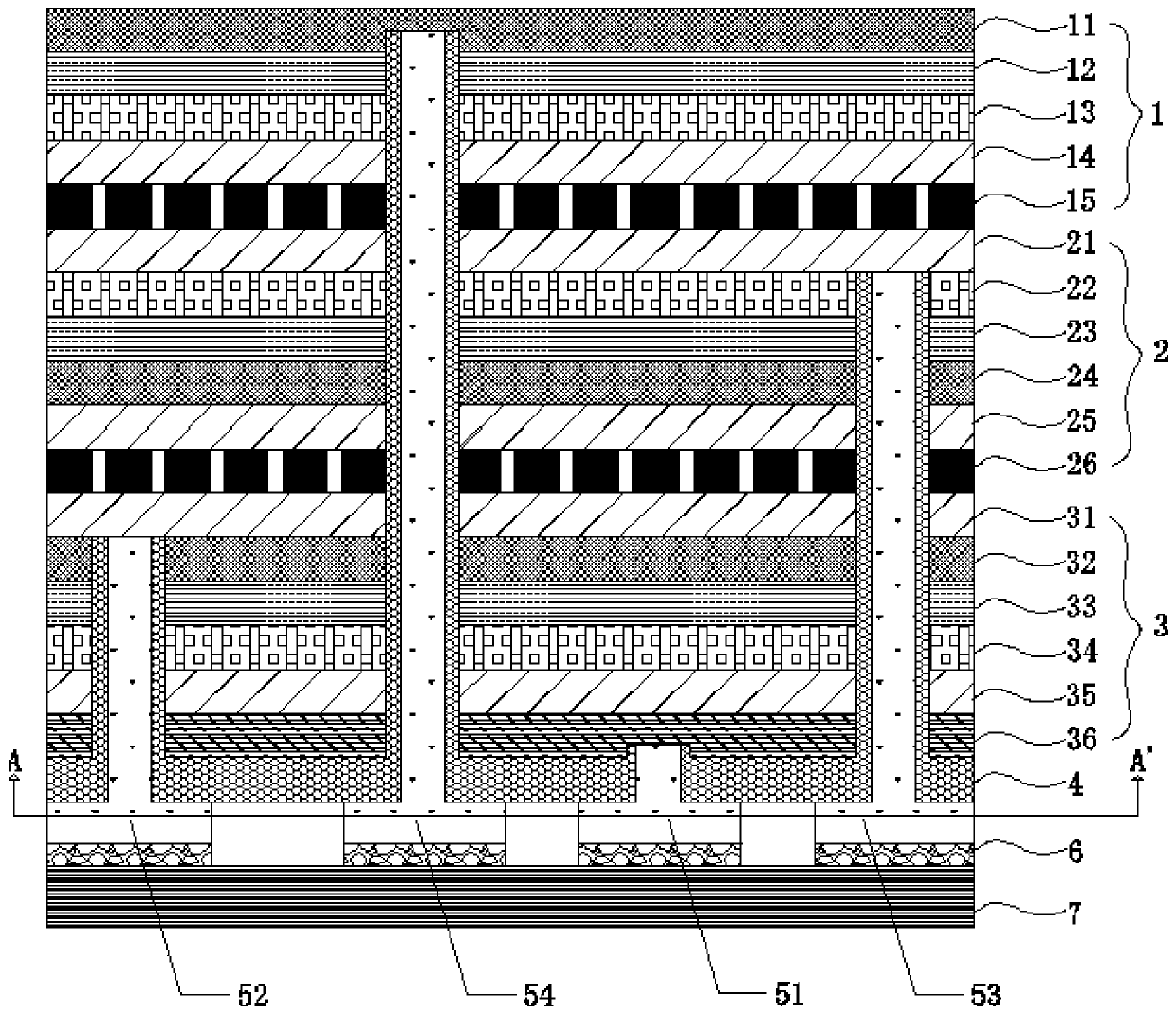
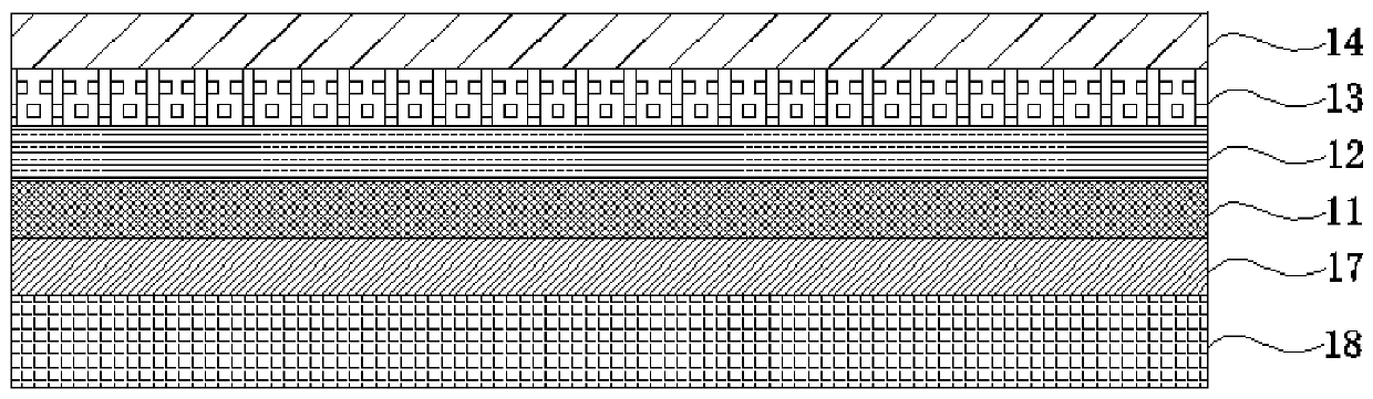
[0049] This embodiment provides a Micro-LED chip, such as figure 1 , figure 2 shown, including:

[0050] Carrier 7;

[0051] Several light-emitting units connected to the carrier plate 7 through the bonding layer 6, each light-emitting unit includes an electrode group, an isolation layer 4, a third LED stack 3, a second LED stack 2, The first LED stack 1; the second LED stack 2 is electrically connected to the third LED stack 3 through the conductive channel; the first LED stack 1 is electrically connected to the second LED st...


PUM


Abstract

The invention provides a comprises a Micro-LED chip, a display device and a manufacturing method of micro-LED chip. The Micro-LED chip comprises a carrier plate and a plurality of light-emitting units connected with the carrier plate. Each light-emitting unit comprises an electrode group, an isolation layer, a third LED stack, a second LED stack and a first LED stack, wherein the electrode group, the isolation layer, the third LED stack, the second LED stack and the first LED stack are sequentially arranged on the surface of the carrier plate; the second LED stack is electrically connected with the third LED stack through a conductive channel; and the first LED stack is electrically connected with the second LED stack through a conductive channel. By configuring different material systems of the third LED stacks, the second LED stacks and the first LED stacks and combining a driving circuit to control the on / off of a first electrode bonding pad, a second electrode bonding pad, a third electrode bonding pad and a fourth electrode bonding pad and the magnitude of input current, a plurality of light emitting modes of independent control and color mixing control of a plurality of primary colors are realized, and light emitting of full light systems can be achieved only through one Micro-LED chip.

Description

technical field [0001] The present application relates to the field of semiconductor technology, and more specifically, to a Micro-LED chip, a display device, and a method for manufacturing the Micro-LED chip. Background technique [0002] Micro-LED has developed into one of the hot spots of future display technology, but its technology is difficult and complicated. Generally, the traditional RGB uses three-color micro-light-emitting element arrays to transfer to the receiving substrate, and three RGB elements in each group are gathered together to form an RGB effect. However, after entering Micro-LED technology: firstly, the process of mass transfer and mixing each group of RGB is too complicated, resulting in low mass production yield, high production cost, and long time-consuming; secondly, due to the sub-pixel It is located in the two-dimensional plane of the display device, so the area occupied by one pixel is relatively large, including sub-pixels for blue light, gree...

Claims


Application Information

Patent Timeline
IPC IPC(8): H01L33/62H01L33/10H01L25/075G09F9/33
CPCH01L33/62H01L33/10H01L25/0756G09F9/33H01L2933/0066
Inventor 林志伟陈凯轩曲晓东蔡建九柯志杰
Owner XIAMEN QIANZHAO SEMICON TECH CO LTD
Why Eureka
Try Eureka