Soldering process capable of regulating and controlling grain orientation and structure of tin soldered joint

A technology of grain orientation and welding process, applied in welding equipment, manufacturing tools, metal processing equipment, etc., can solve the problems of poor grain orientation, failure, complex service environment of solder joints, etc., to achieve improved reliability and practicability Strong, fewer welding process steps

Inactive Publication Date: 2019-09-03
BEIJING INSTITUTE OF TECHNOLOGYGY
View PDF8 Cites 5 Cited by
  • Summary
  • Abstract
  • Description
  • Claims
  • Application Information

AI Technical Summary

Problems solved by technology

[0005] However, the actual service environment of solder joints is very complicated, and it faces failures caused by various reasons such as electromigration, thermal migration, thermomechanical fatigue and mechanical fatigue, so it is difficult to determine what kind of solder joints have in specific working environments. Specific grain orientation has the longest service life, however, it is still effective to improve the reliability of solder joints by controlling grain orientation
On the one hand, the grain orientation of the solder joints prepared by the traditional process is random. Since electronic devices often contain a large number of solder joints, compared with the solder joints whose grain orientation is controlled, the grain orientation of the traditional process is solder joints are more prone to have poor grain orientation, causing failure

Method used


Image

  • Soldering process capable of regulating and controlling grain orientation and structure of tin soldered joint
  • Soldering process capable of regulating and controlling grain orientation and structure of tin soldered joint
  • Soldering process capable of regulating and controlling grain orientation and structure of tin soldered joint

Examples


Embodiment 1

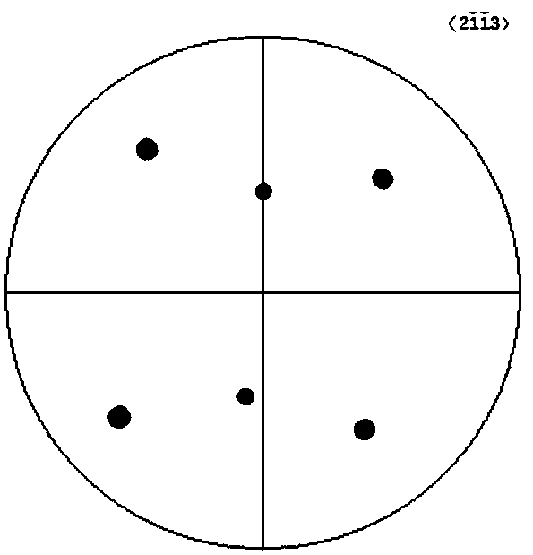
[0027] Step 1: Make 8 pads on the resin-based PCB, and deposit a layer of Co single crystal with a thickness of 10um by physical vapor deposition at each pad position. The pole figure of Co single crystal is as follows figure 1 shown;

[0028] Step 2: Uniformly coat a layer of flux on each deposited Co single crystal pad, and fix a solder ball with a diameter of 500 μm and a purity of 99.99% on the single crystal metal;

[0029] Step 3: Heat the heating plate to 300°C at a heating rate of 30°C / min. Place the resin-based PCB flat on the heating plate and keep it warm for 100s. Then clamp the PCB away from the heating plate and cool to room temperature. The welding is complete.

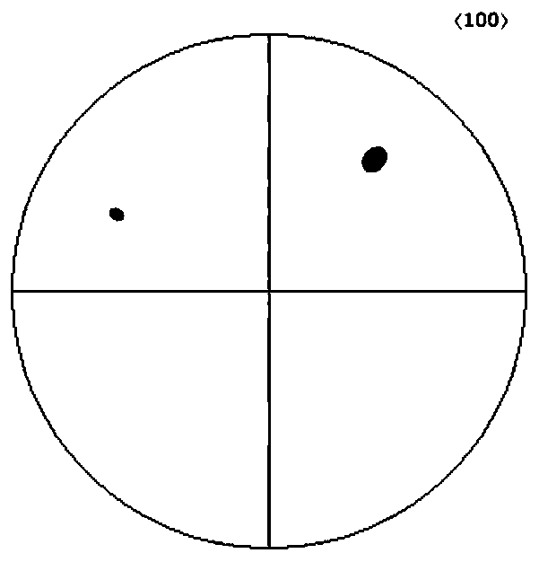
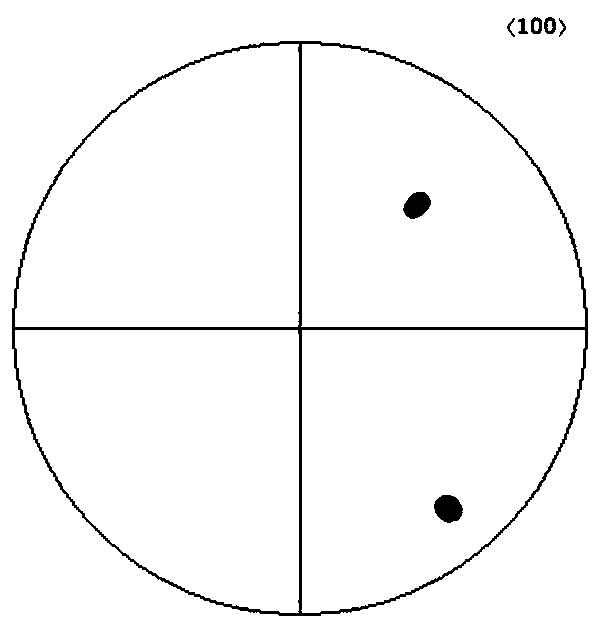
[0030] Electron backscattering (EBSD) tests were carried out on the 10 solder joints in the PCB boards soldered in step 3. The interface intermetallic compound CoSn in the first solder joint 3 The polar figure such as figure 2 As shown, the pole figure of βSn in the solder joint is as follows image...

Embodiment 2

[0032] Step 1: Deposit a layer of Pd single crystal with a thickness of 15um on the 5 pads of the resin-based PCB by physical vapor deposition;

[0033] Step 2: Uniformly coat a layer of flux on the deposited Pd single crystal, and fix SnAgCu solder balls with a diameter of 500 μm on the single crystal metal;

[0034] Step 3: Heat up the reflow soldering machine to 280°C with a heating rate of 40°C / min, place the single crystal substrate in the reflow soldering machine, keep it warm for 90s, take out the PCB board, and cool it to room temperature with the air, and the soldering is complete.

[0035] Perform EBSD tests on the 5 solder joints on the PCB board that have been soldered in step 3, and the pole figures are as follows Figure 4 As shown, the test results show that the measured solder joints are single crystal, and the grain orientation of βSn is obviously controlled.

Embodiment 3

[0037] Step 1: Deposit a layer of Co single crystal with a thickness of 15um on the 5 pads of the resin-based PCB by physical vapor deposition;

[0038] Step 2: uniformly coat a layer of flux on the deposited Co single crystal, and fix a solder ball with a diameter of 500 μm and a purity of 99.99% on the single crystal metal;

[0039] Step 3: Heat up the reflow soldering machine to 300°C with a heating rate of 60°C / min, put the resin-based PCB board in the reflow soldering machine, keep it warm for 80s, take out the PCB board, and cool it to room temperature with the air, and the soldering is completed.

[0040] The characterization of the experimental results: such as Figure 5 Scanning electron microscope (SEM) pictures found that due to the influence of the Co single crystal substrate, the intermetallic compounds in the measured solder joints have obvious specific orientations, and the angle between the two specific orientations is 90°.


PUM

PropertyMeasurementUnit
diameteraaaaaaaaaa

Abstract

The invention relates to a soldering process capable of regulating and controlling the grain orientation and structure of a tin soldered joint. The soldering process comprises the following steps thatfirstly, a layer of single crystal metal material is deposited at the position of each bonding pad of a PCB with a physical or chemical or electrochemical method or single crystal metal material protrusion points are grown on the surface of a wafer; secondly, oxides and organic contaminants on the surface of the single crystal metal material are removed; thirdly, tin-based soldering flux is soldered to the single crystal metal material with a brazing technology, and then the tin soldered joint with the specific grain orientation and structure is obtained. Since the grain orientation and structure of the tin soldered joint are effectively controlled, the reliability of the tin soldered joint can be greatly improved.

Description

technical field [0001] The invention relates to a welding process for regulating the grain orientation and structure of solder joints, and belongs to the technical field of electronic packaging. Background technique [0002] With the complexity of the service environment of integrated circuits, the service temperature of electronic devices can reach -40°C-180°C, and they often need to carry high currents, even accompanied by severe vibrations and shocks. As an extremely important part of electronic interconnection, solder joints play an irreplaceable role in mechanical connection and electrical signal transmission. They often face extremely serious failures such as electromigration, thermal migration, thermal fatigue, and mechanical fatigue. lead to overall failure of the device. [0003] The study found that the reason for the above failure is related to the βSn structure and grain orientation in the solder joint. In the traditional soldering process, before soldering, al...

Claims


Application Information

Patent Timeline
Patent Type & Authority Applications(China)
IPC IPC(8): B23K1/00B23K1/08B23K1/20
CPCB23K1/0008B23K1/08B23K1/20
Inventor 马兆龙李策程兴旺
Owner BEIJING INSTITUTE OF TECHNOLOGYGY
Why Eureka
Try Eureka