A pogo pin test connector suitable for semiconductor wafer fabrication

A technology for testing connectors and pogo pins, which is applied in semiconductor/solid-state device testing/measurement, instruments, measuring devices, etc., and can solve problems such as misalignment and affecting test results

Active Publication Date: 2021-03-26
东莞市精端精密五金制品有限公司
View PDF6 Cites 0 Cited by
  • Summary
  • Abstract
  • Description
  • Claims
  • Application Information

AI Technical Summary

Problems solved by technology

[0006] In order to solve the problem that the pogo pin of the above technology is round and smooth, when it is placed on a wafer with a little water mist for testing, it will slide a little when it is fixed, which will easily cause its misalignment and affect the test results.

Method used


Image

  • A pogo pin test connector suitable for semiconductor wafer fabrication
  • A pogo pin test connector suitable for semiconductor wafer fabrication
  • A pogo pin test connector suitable for semiconductor wafer fabrication

Examples


Embodiment

[0030] as attached figure 1 to attach Figure 8 Shown:

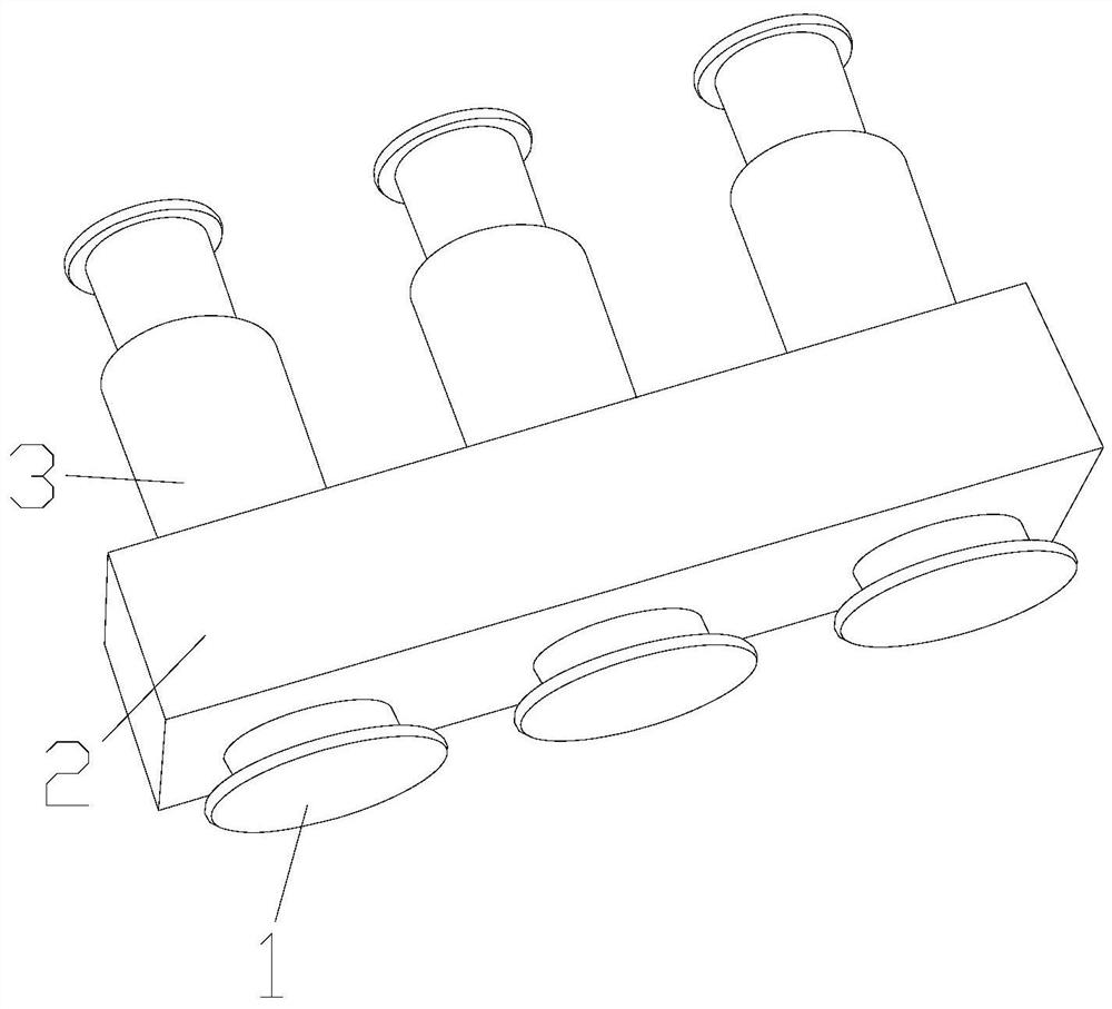
[0031] The invention provides a pogo pin test connector suitable for manufacturing semiconductor wafers, the structure of which includes a spring top 1 , a connector 2 and an anti-slip pogo pin 3 .

[0032] The spring top 1 and the anti-slip pogo pin 3 are an integrated structure, the anti-slip pogo pin 3 penetrates inside the connector 2 , and the spring top 1 is embedded in the inside of the connector 2 .

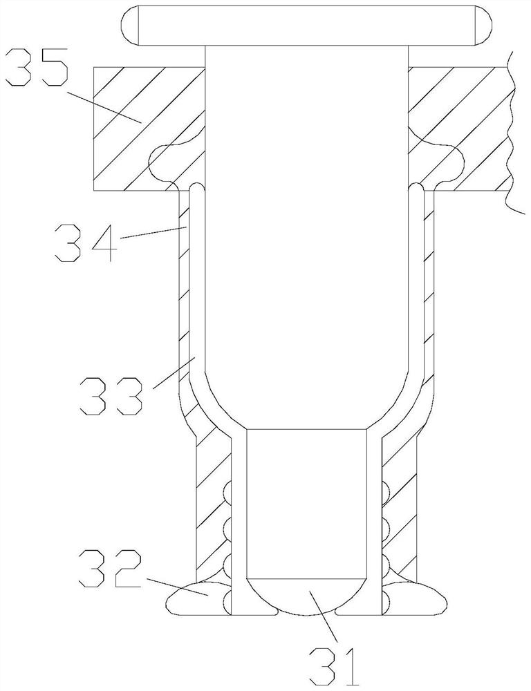
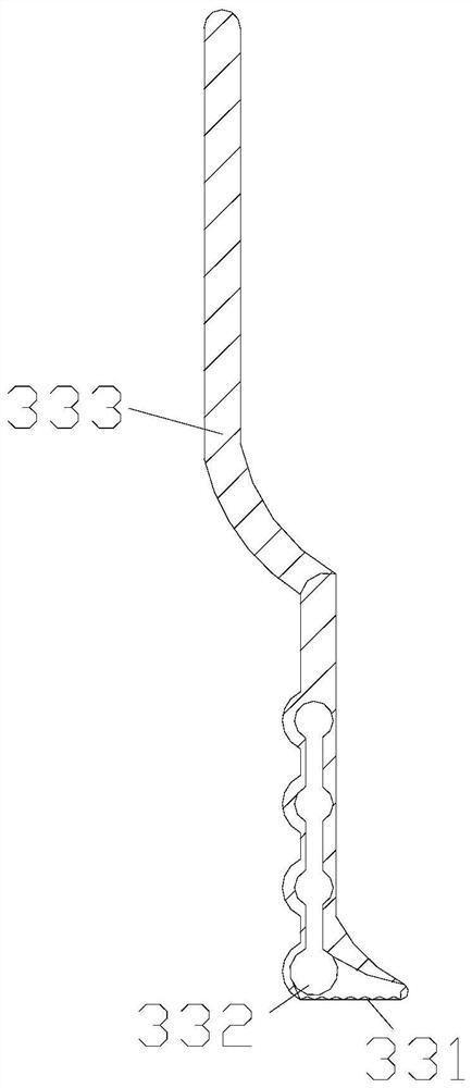
[0033] The anti-slip pogo pin 3 includes a test round head 31, a suction disc 32, an inner suction strip 33, a card layer 34, and an interlayer 35. The test round head 31 is located between the adsorption discs 32, and the inner suction strip 33 is installed on the Between the card layer 34 and the test round head 31 , the card layer 34 is embedded in the interlayer 35 , and the test round head 31 is arranged between the interlayer 35 .

[0034] Wherein, the internal suction strip 33 includes a main water-absorbi...


PUM


Abstract

The invention discloses a pogo pin test connector suitable for manufacturing semiconductor wafers. The structure includes a spring top, a connector, and an anti-slip pogo pin. The spring top and the anti-slip pogo pin are an integrated structure. The anti-slip pogo pin includes a test round head , inner suction strip, card layer, and compartment. The test round head is located between the adsorption plates. When the connector is to test the wafer, the main water absorption layer absorbs the surrounding water mist, so that it can be sucked into the inner layer. The sticky ball will touch the object first, and the stabilizing angle will touch the surface, pushing its inner core inward, and its power transmission arc will be pressed inward by force, and the airbag above the force transmission arc will be stressed, The booster strut located on the surface of the suction bag will be stressed together and spread out to both sides, making the sticky ball stretch inside the expanded groove, allowing the suction plate to adhere more firmly, which can make the pogo pin more fixed and accurate Test it properly without letting it slip or even dislocate, so as to prevent the test effect from being affected.

Description

technical field [0001] The invention belongs to the field of semiconductors, and more specifically relates to a pogo pin test connector suitable for manufacturing semiconductor wafers. Background technique [0002] When semiconductor wafers are manufactured in Nanfengtian, a little fog will adhere to the surface. After the wafers are manufactured, they need to be inspected through pogo pin connectors to prevent some problems in mass production and delay follow-up work. [0003] Based on the above-mentioned inventor's discovery, the existing semiconductor wafer manufacturing pogo pin test connector mainly has the following deficiencies, such as: [0004] The pogo pin has a round head shape and is relatively smooth. When it is placed on a wafer with a little water mist for testing, it will slide a little when it is fixed, which will easily cause its misalignment and affect the test results. [0005] Therefore, it is necessary to propose a pogo pin test connector suitable for ...

Claims


Application Information

Patent Timeline
Patent Type & Authority Patents(China)
IPC IPC(8): H01L21/66G01R1/04
CPCG01R1/0416H01L22/30
Inventor 谢继娇彭鸿琦
Owner 东莞市精端精密五金制品有限公司
Why Eureka
Try Eureka