Thin-film photovoltaic cell and manufacturing method thereof
A technology of thin-film photovoltaic cells and manufacturing methods, which is applied in photovoltaic power generation, circuits, electrical components, etc., can solve the problems of inability to obtain integrated black display effect and reduce consumer experience, and achieve the effect of reducing optical interference and good display effect
- Summary
- Abstract
- Description
- Claims
- Application Information
AI Technical Summary
Problems solved by technology
Method used
Image
Examples
Embodiment 1
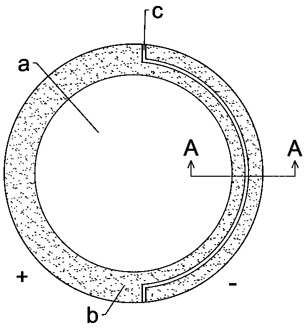
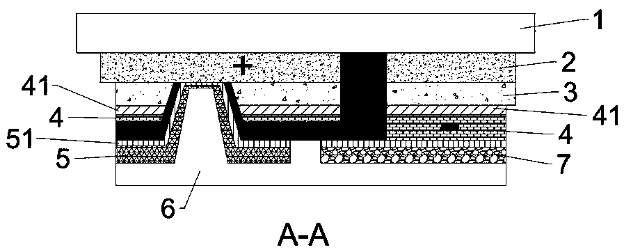
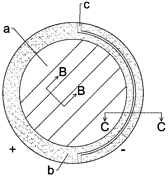
[0032] combine figure 1 , figure 2 As shown, the embodiment of the present invention provides a thin film photovoltaic cell, including a transparent substrate 1 and a photovoltaic unit arranged on the transparent substrate 1 and facing the electronic display module, and the photovoltaic unit includes a photovoltaic unit arranged on the transparent substrate 1 The front electrode 2, the light absorbing layer 3 arranged on the front electrode 2 and the back electrode 4 arranged on the light absorbing layer 3, the surface of the back electrode 4 facing the transparent substrate 1 is provided with a first blackened metal Conductive layer 41, the arrangement of the first blackened metal conductive layer 41 makes the overall color of the photovoltaic unit closer to the color of the electronic display module, and realizes the integrated black effect of the thin film photovoltaic cell and the electronic display module.
[0033] Further, the thin-film photovoltaic cell also includes ...
Embodiment 2
[0047] Embodiment 2 of the present invention provides the manufacturing method of the thin-film photovoltaic cell described in Embodiment 1, comprising the following steps:
[0048] S1: Provide a transparent substrate 1, and perform film formation, imaging, and etching of the front electrode 2 on the side of the transparent substrate 1 facing the electronic display module.
[0049] S2: Forming, imaging and etching the light absorbing layer 3 on the side of the front electrode 2 facing the electronic display module.
[0050] S3: Depositing the first blackened metal conductive layer 41 on the side of the light absorbing layer 3 facing the electronic display module.
[0051] S4: Perform film formation, imaging, and etching of the back electrode 4 on the side of the first blackened metal conductive layer 41 facing the electronic display module.
[0052] The thin-film photovoltaic cell manufacturing method described in the embodiment of the present invention deposits the first bla...
PUM
 Abstract
Description
Claims
Application Information
 - R&D
- Intellectual Property
- Life Sciences
- Materials
- Tech Scout
- Unparalleled Data Quality
- Higher Quality Content
- 60% Fewer Hallucinations
Browse by: Latest US Patents, China's latest patents, Technical Efficacy Thesaurus, Application Domain, Technology Topic, Popular Technical Reports.
© 2025 PatSnap. All rights reserved.Legal|Privacy policy|Modern Slavery Act Transparency Statement|Sitemap|About US| Contact US: help@patsnap.com


