


Quick Research
Generate reliable direction feasibility study reports for your R&D in just a few steps.

Technical Q&A
Discover and master advanced knowledge NOW. Basics, ideas, possibilities, all at once.

Find Solutions
As an expert in R&D theories, this can generate solutions to your technical problems instantly.

Evaluate Feasibility
Analyze your overall solution with one click, know your potential R&D risks in advance.

Monitor Landscape
Get weekly tech updates, stay abreast of the latest tech innovations and key insights.
Manufacturing method of thin film touch sensor and thin film touch sensor
A technology of touch sensing and manufacturing methods, which is applied in the input/output process of instruments, data processing, electrical digital data processing, etc., and can solve the problem of stacking offset of each layer of lines, small stacking offset of lines, and exposure alignment efficiency Low-level problems, to achieve the effect of small line stack offset, accurate exposure alignment, stable and controllable shape and size changes
- Summary
- Abstract
- Description
- Claims
- Application Information
AI Technical Summary
Problems solved by technology
Method used
Image

Examples
Embodiment 1
[0068] A method for manufacturing a thin film touch sensor, comprising the following steps:
[0069] (a) Bake the rigid carrier plate coated with the film base material, the baking temperature is 130°C, and the baking time is 60 minutes; the film base material is a PET film base material, the rigid carrier plate is a glass plate, and the film base material is a glass plate. The bonding glue between the material and the rigid carrier is acrylic glue;
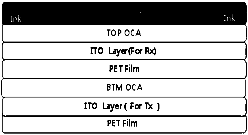
[0070] (b) Make multi-layer touch circuit:
[0071] The first ITO coating;
[0072] The first ITO circuit process: photoresist coating, soft baking, exposure, development, hard baking, etching, and photoresist stripping. The soft baking temperature is 110°C. After baking, let it stand for 3 minutes, and the temperature of the exposure table is controlled at 25°C;
[0073] The first OC line process: OC photoresist coating, soft baking, exposure, development and curing, the soft baking temperature is 110 °C, the soft baking time ...
Embodiment 2
[0081] A manufacturing method of a thin-film touch sensor differs from Embodiment 1 in that the baking temperature is 140° C. and the baking time is 40 minutes, and other steps and parameters thereof are the same as Embodiment 1.
Embodiment 3
[0083] A manufacturing method of a thin-film touch sensor is different from Embodiment 1 in that the baking temperature is 120° C. and the baking time is 60 minutes, and other steps and parameters thereof are the same as Embodiment 1.
PUM
 Abstract
Description
Claims
Application Information
 - R&D Engineer
- R&D Manager
- IP Professional
- Industry Leading Data Capabilities
- Powerful AI technology
- Patent DNA Extraction
Browse by: Latest US Patents, China's latest patents, Technical Efficacy Thesaurus, Application Domain, Technology Topic, Popular Technical Reports.
© 2024 PatSnap. All rights reserved.Legal|Privacy policy|Modern Slavery Act Transparency Statement|Sitemap|About US| Contact US: help@patsnap.com