


Quick Research
Generate reliable direction feasibility study reports for your R&D in just a few steps.

Technical Q&A
Discover and master advanced knowledge NOW. Basics, ideas, possibilities, all at once.

Find Solutions
As an expert in R&D theories, this can generate solutions to your technical problems instantly.

Evaluate Feasibility
Analyze your overall solution with one click, know your potential R&D risks in advance.

Monitor Landscape
Get weekly tech updates, stay abreast of the latest tech innovations and key insights.
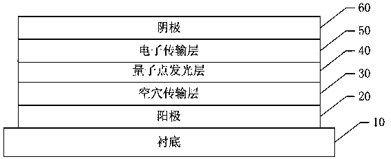
A kind of nanometer material and preparation method thereof, optoelectronic device
A technology for optoelectronic devices and nanomaterials, applied in the fields of electrical solid devices, nanotechnology, electrical components, etc., can solve the problems of high cost, complex preparation process, low hole injection efficiency, etc., to improve luminous efficiency and performance, improve air The effect of hole transport efficiency and improving migration efficiency
- Summary
- Abstract
- Description
- Claims
- Application Information
AI Technical Summary
Problems solved by technology
Method used
Image

Examples
preparation example Construction
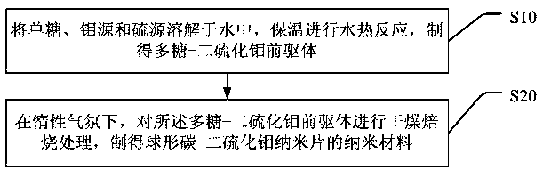
[0024] see figure 1 , figure 1 A flow chart of a preferred embodiment of a nanomaterial preparation method provided by the present invention, as shown in the figure, includes steps:
[0025] S10, dissolving monosaccharide, molybdenum source and sulfur source in water, keeping warm for hydrothermal reaction, and preparing polysaccharide-molybdenum disulfide precursor;
[0026] S20. Drying and calcining the polysaccharide-molybdenum disulfide precursor under an inert atmosphere to prepare spherical carbon-molybdenum disulfide nanosheet nanomaterials.
[0027] In this embodiment, the monosaccharide is dehydrated and polycondensed into a polysaccharide template under hydrothermal conditions, and the space confinement effect of the polysaccharide in situ template can effectively confine MoS 2 Growth of nanosheets in the crystal c-direction to generate ultrathin MoS 2 Nanosheets.
[0028] Specifically, the molybdenum source and the sulfur source generate MoS under hydrothermal c...
Embodiment 1
[0044] 1, the preparation method of nanometer material comprises steps:
[0045] 1) Dissolve 1g of glucose, 0.1g of ammonium molybdate and 0.25g of ammonium sulfide into 20ml of water;
[0046] 2) After the glucose, ammonium molybdate and ammonium sulfide are completely dissolved, transfer them to the hydrothermal reaction kettle. o C for 24h, cooled and washed (washed twice with water, washed once with absolute ethanol), and then at 50 o Dry at C to prepare MoS 2 / polysaccharide precursor;
[0047] 3), the MoS 2 / The polysaccharide precursor was heated to 800 °C under an Ar atmosphere o C was calcined for 5 hours to obtain carbon-molybdenum disulfide nanomaterials.
[0048] 2. Application of nanomaterials:
[0049] 1) Dissolve the carbon-molybdenum disulfide nanomaterial in 10ml of NMP, and disperse it ultrasonically to form a carbon-molybdenum disulfide hybrid nano solution of about 0.8M~1M;
[0050] 2) Spin-coat the carbon-molybdenum disulfide hybrid nano solution ...
Embodiment 2
[0053] 1, the preparation method of nanometer material comprises steps:
[0054] 1) Dissolve 1g fructose, 0.1g sodium molybdate and 0.25g thiourea into 20ml water;
[0055] 2) After the fructose, sodium molybdate and thiourea are completely dissolved, transfer them to the hydrothermal reaction kettle. o C for 26h, cooled and washed (washed twice with water, washed once with absolute ethanol), and then at 50 o Dry at C to prepare MoS 2 / polysaccharide precursor;
[0056] 3), the MoS 2 / Polysaccharide precursor was heated to 850C and roasted for 4h under Ar atmosphere to prepare carbon-molybdenum disulfide nanomaterials.
[0057] 2. Application of nanomaterials:
[0058] 1) Dissolve the carbon-molybdenum disulfide nanomaterial in 10ml DMSO, and disperse it ultrasonically to form a carbon-molybdenum disulfide hybrid nano solution of about 0.8M~1M;
[0059] 2) Spin-coat the carbon-molybdenum disulfide hybrid nano solution onto the ITO substrate at 200-300 o C annealing and...
PUM
 Abstract
Description
Claims
Application Information
 - R&D Engineer
- R&D Manager
- IP Professional
- Industry Leading Data Capabilities
- Powerful AI technology
- Patent DNA Extraction
Browse by: Latest US Patents, China's latest patents, Technical Efficacy Thesaurus, Application Domain, Technology Topic, Popular Technical Reports.
© 2024 PatSnap. All rights reserved.Legal|Privacy policy|Modern Slavery Act Transparency Statement|Sitemap|About US| Contact US: help@patsnap.com