
Package for chip scale magnetometer or atomic clock

An atomic clock, a chip-sized technology that is applied to instruments using atomic clocks, electrodynamic magnetometers, magnitude/direction of magnetic fields, etc., can solve problems such as attempts to hinder measurement sensitivity

Inactive Publication Date: 2019-06-28
TEXAS INSTR INC
View PDF7 Cites 0 Cited by
  • Summary
  • Abstract
  • Description
  • Claims
  • Application Information

AI Technical Summary

Problems solved by technology

Inherent noise in the system can hinder attempts to increase measurement sensitivity

Method used


Image

  • Package for chip scale magnetometer or atomic clock
  • Package for chip scale magnetometer or atomic clock
  • Package for chip scale magnetometer or atomic clock

Examples


Embodiment Construction

[0013] In the drawings, like references indicate similar elements. In this description, the term "couple / couples" means an indirect or direct electrical connection, unless defined as being "communicatively coupled," which may include a wireless connection. Thus, if a first device couples to a second device, that connection may be through a direct electrical connection or through an indirect electrical connection via other devices and connections.

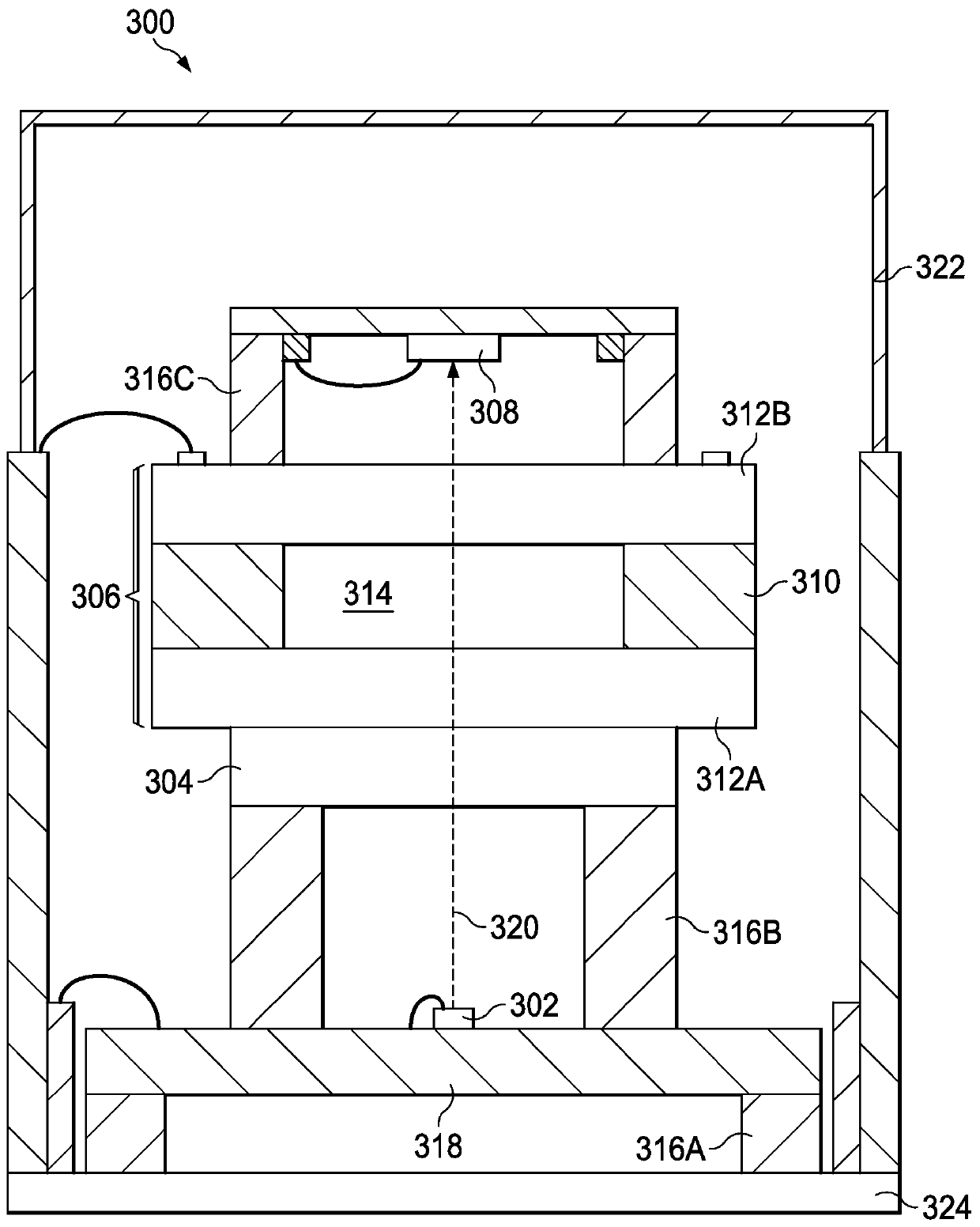
[0014] FIG. 3 is a block diagram of a conventional package 300 for a CSAC or magnetometer. Package 300 contains a laser 302 , a vapor chamber 306 enclosing the alkali metal vapor, and a photodetector 308 . Laser 302 may be a vertical-cavity surface-emitting laser (VCSEL) arranged to send a beam 320 through vapor chamber 306 at a predetermined frequency and provide beam 320 to light detector 308 . In one example, vapor chamber 306 contains Cs 133 , while the laser 302 is tuned to 894nm. Optical package 304 may be placed between l...


PUM


Abstract

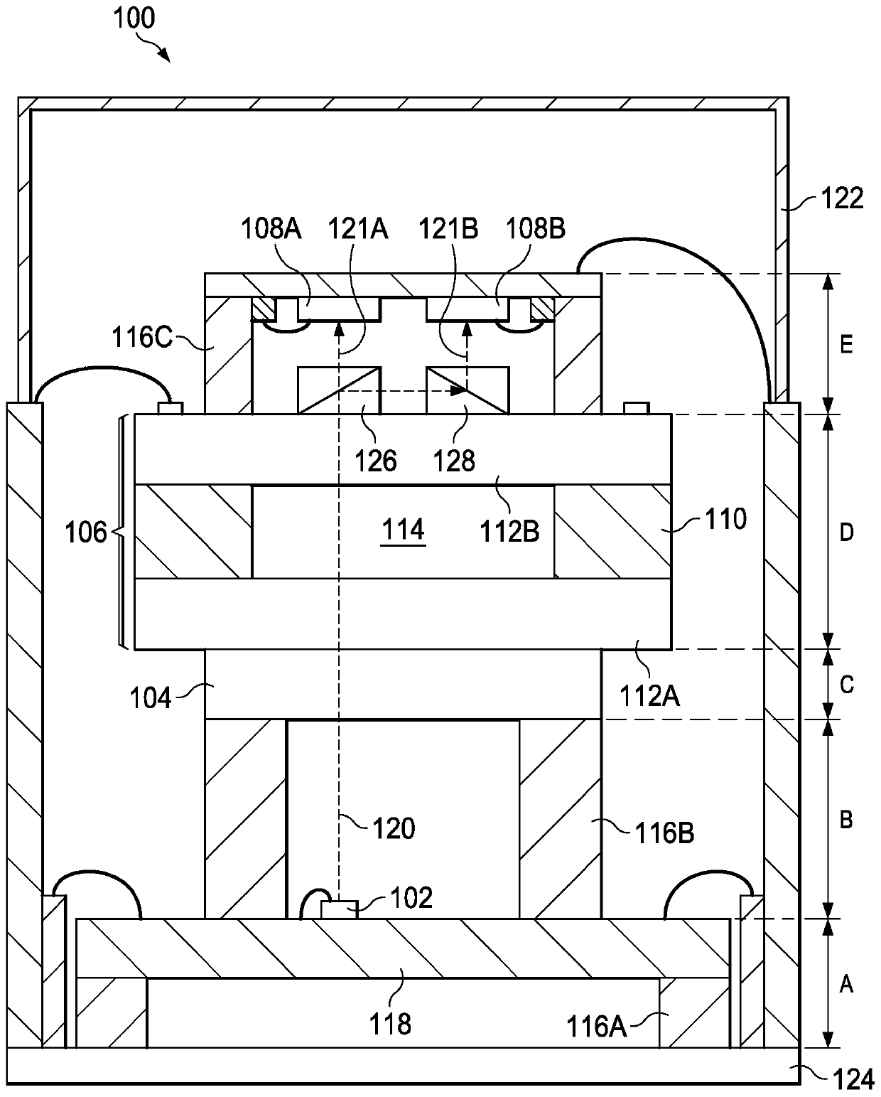
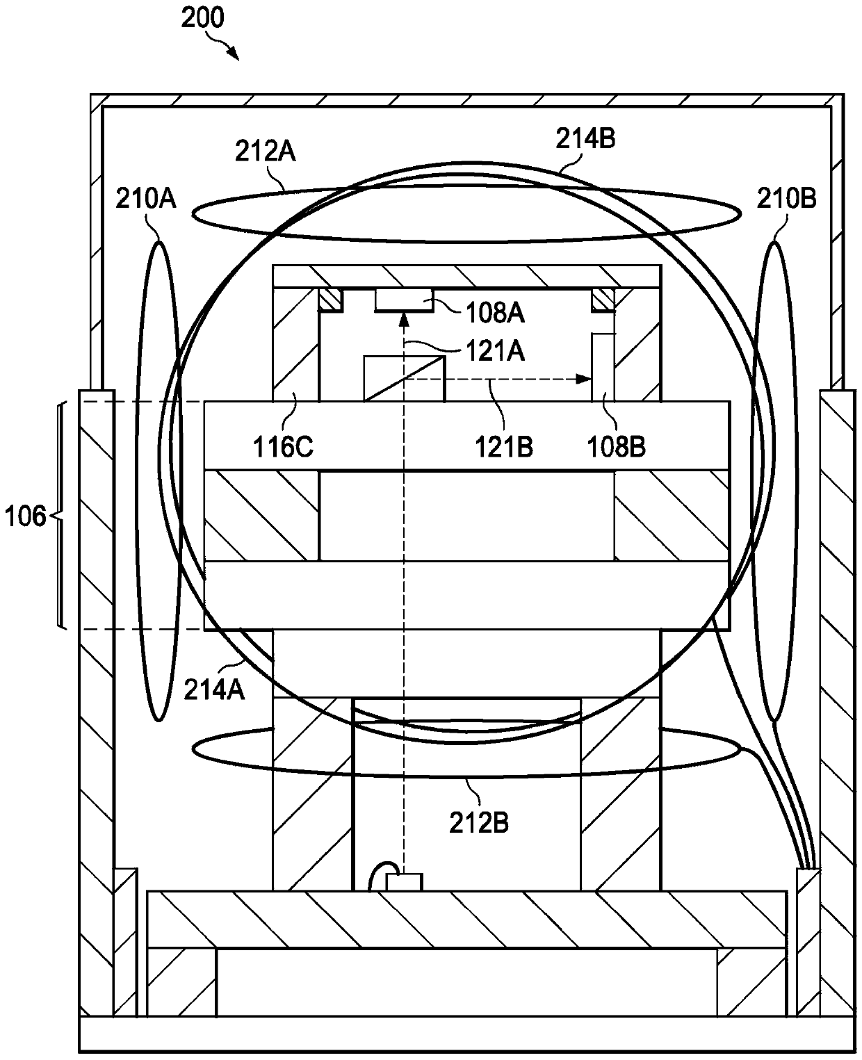
In described examples of a package (200) for a chip scale atomic clock or magnetometer, the package (200) includes a vapor cell using an alkali metal vapor, first and second photodetectors (108A, 108B), and a laser operable at a frequency that excites an electron transition in the alkali metal vapor. The laser is positioned to provide an optical signal directed through the vapor cell and towards the first photodetector (108A). The package (200) further contains a polarizing beam splitter, which is positioned between the vapor cell and the first photodetector (108A) to receive the optical signal and to split the optical signal into a first signal (121A) directed toward the first photodetector (108A) and a second signal (121B) directed toward the second photodetector (108B). The first signal(121A) is orthogonal to the second signal (121B).

Description

[0001] The present invention relates generally to packaging semiconductor chips, and more particularly to packaging for magnetometers or atomic clocks. Background technique [0002] Both chip-scale atomic clocks (CSACs) and magnetometers use vapor cells enclosing a vapor of an alkali metal, usually rubidium (Rb) or cesium (Cs). A laser sends a signal at optical wavelengths through the vapor chamber, exciting hyperfine transitions using a phenomenon known as coherent population trapping (CPT). For example, a cesium-based CSAC may use a laser tuned to the D1 absorption line of cesium at 894 nm. The laser scans a frequency region around the absorption line and the amount of light absorbed while passing through the vapor chamber is monitored at a photodetector. A region of maximum absorption is detected and used to stabilize the reference frequency provided by the CSAC or magnetometer. Inherent noise in the system can hinder attempts to improve measurement sensitivity. [0003]...

Claims


Application Information

Patent Timeline
Patent Type & Authority Applications(China)
IPC IPC(8): G04F5/14G01R33/028B81B7/02
CPCB81B7/0032B81B7/02G04F5/14G01R33/028G01R33/032H03B17/00
Inventor 胡安·赫布佐默本杰明·库克
Owner TEXAS INSTR INC
Learn More