
Shift register, gate drive circuit, display device and gate driving method

A shift register, reset circuit technology, applied in the field of gate drive circuit, shift register, gate drive, can solve the problem of large number and disadvantageous narrow frame realization, etc.

Active Publication Date: 2019-06-28
BOE TECH GRP CO LTD +1
View PDF5 Cites 18 Cited by
  • Summary
  • Abstract
  • Description
  • Claims
  • Application Information

AI Technical Summary

Problems solved by technology

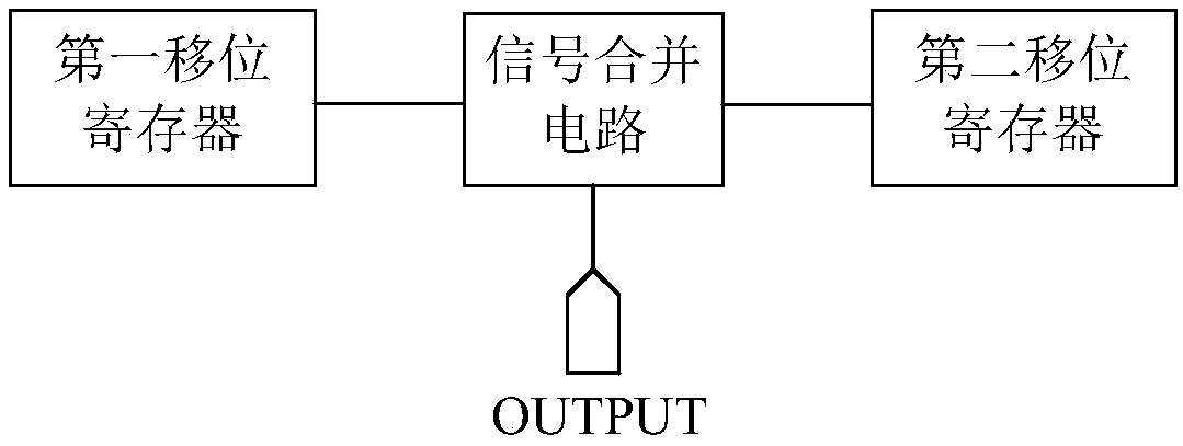
However, the gate drive unit includes two shift registers and a signal combining circuit, which requires a large number of TFTs, which is not conducive to the realization of narrow borders.

Method used


Image

  • Shift register, gate drive circuit, display device and gate driving method
  • Shift register, gate drive circuit, display device and gate driving method
  • Shift register, gate drive circuit, display device and gate driving method

Examples


Embodiment Construction

[0083] In order for those skilled in the art to better understand the technical solution of the present invention, a shift register, a gate driving circuit, a display device and a gate driving method provided by the present invention will be described in detail below with reference to the accompanying drawings.

[0084] It should be noted that the transistors in the present invention may be thin film transistors or field effect transistors or other switching devices with the same characteristics. A transistor generally includes three poles: a gate, a source, and a drain. The source and drain in a transistor are symmetrical in structure, and the two can be interchanged as needed. In the present invention, the gate electrode refers to the gate of the transistor, one of the first electrode and the second electrode is the source, and the other is the drain.

[0085] In addition, according to the characteristics of transistors, transistors can be divided into N-type transistors and...


PUM


Abstract

The invention discloses a shift register, a gate drive circuit, a display device and a gate driving method. The shift register comprises: a display pre-charge reset circuit, a sensing cascade circuit,a sensing pre-charge reset circuit, a reverse circuit and an output circuit. The sensing cascade circuit, the display pre-charge reset circuit, and the sensing pre-charge reset circuit are connectedwith the same reverse circuit and the same output circuit. The output circuit is connected with a plurality of signal output ends. The output circuit comprises a plurality of output sub-circuits in one-to-one correspondence with the signal output ends, and the output sub-circuits are used for writing driving clock signals provided by the driving clock signal ends into the corresponding signal output ends in response to voltage control of pull-up nodes in an effective level state in a display output stage and a sensing output stage. According to the technical scheme, the number of TFTs needingto be set can be effectively reduced while double-pulse driving signals are output.

Description

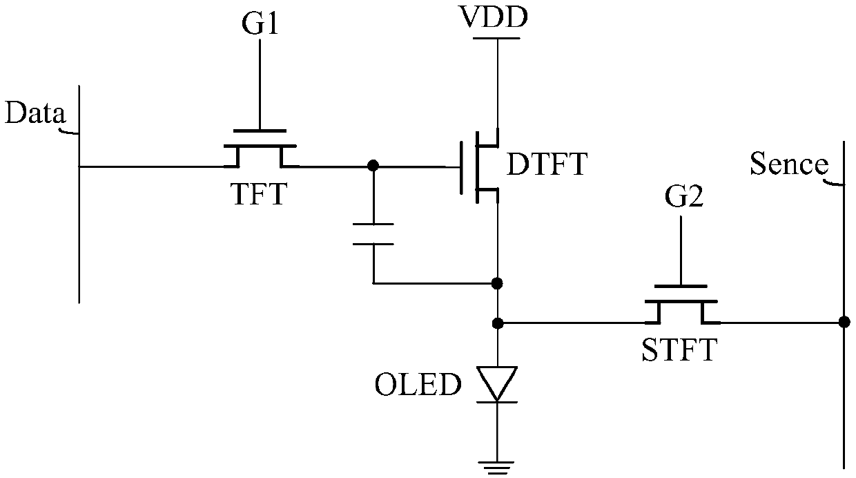
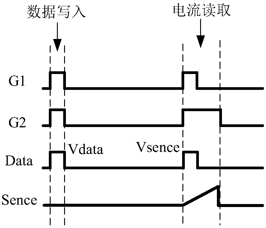
technical field [0001] The invention relates to the field of display technology, in particular to a shift register, a gate drive circuit, a display device and a gate drive method. Background technique [0002] In the prior art, a thin film field effect transistor (Thin Film Transistor, TFT for short) is integrated on the array substrate by using Gate Driver on Array (GOA for short) technology to control the gate lines in the display panel. Scan driving, so that the part of the gate driver IC can be saved, which is conducive to the realization of narrow borders. [0003] For a display panel with an external compensation function, it is required that each gate drive unit in the gate drive circuit (consisting of multiple gate drive units cascaded) can not only output and control the display switching transistor to turn on in the display drive stage The driving signal can also output the driving signal for controlling the conduction of the sensing switching transistor during th...

Claims


Application Information

Patent Timeline
IPC IPC(8): G09G3/3266G11C19/28
CPCG11C19/28G09G3/3266G09G2300/0408G09G2310/0286G09G2310/061G09G2310/066G09G2330/028G09G2320/0295G09G2300/0819
Inventor 冯雪欢李永谦
Owner BOE TECH GRP CO LTD
Learn More