Display substrate, manufacturing method thereof, crack detection method and display device

A display substrate, crack detection technology, applied in identification devices, electronic circuit testing, semiconductor/solid-state device components, etc., can solve the problems of easy to increase the difficulty of wiring in the edge area of ​​the display screen, complicated operations, etc., to reduce the risk of defects , The effect of reducing the difficulty of wiring and increasing the space that can be used for wiring

Active Publication Date: 2019-06-25
BOE TECH GRP CO LTD +1
View PDF5 Cites 29 Cited by
  • Summary
  • Abstract
  • Description
  • Claims
  • Application Information

AI Technical Summary

Problems solved by technology

[0004] The object of the present invention is to provide a display substrate and its manufacturing method, a crack detection method, and a display device, which are used to solve the problem that the existing crack detection method is complicated to operate and easily increases the difficulty of wiring in the edge area of ​​the display screen

Method used


Image

  • Display substrate, manufacturing method thereof, crack detection method and display device
  • Display substrate, manufacturing method thereof, crack detection method and display device
  • Display substrate, manufacturing method thereof, crack detection method and display device

Examples


Embodiment Construction

[0035] In order to further illustrate the display substrate provided by the embodiments of the present invention, the manufacturing method thereof, the crack detection method, and the display device, a detailed description will be given below in conjunction with the accompanying drawings.

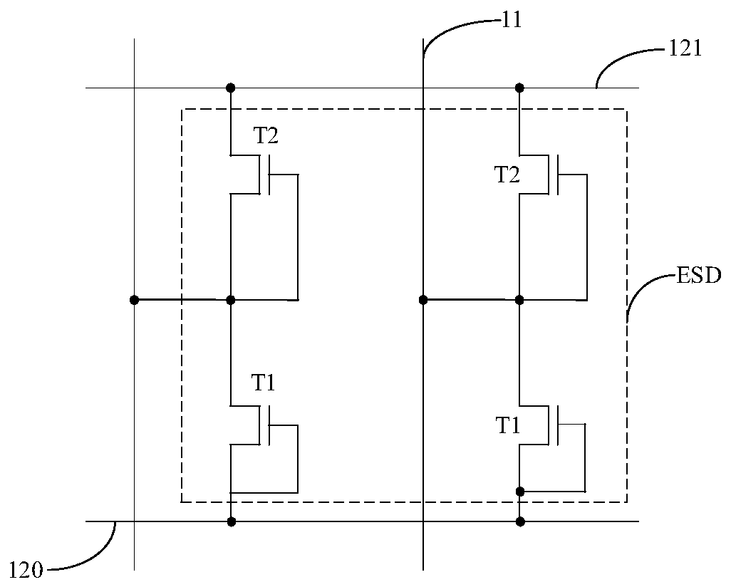
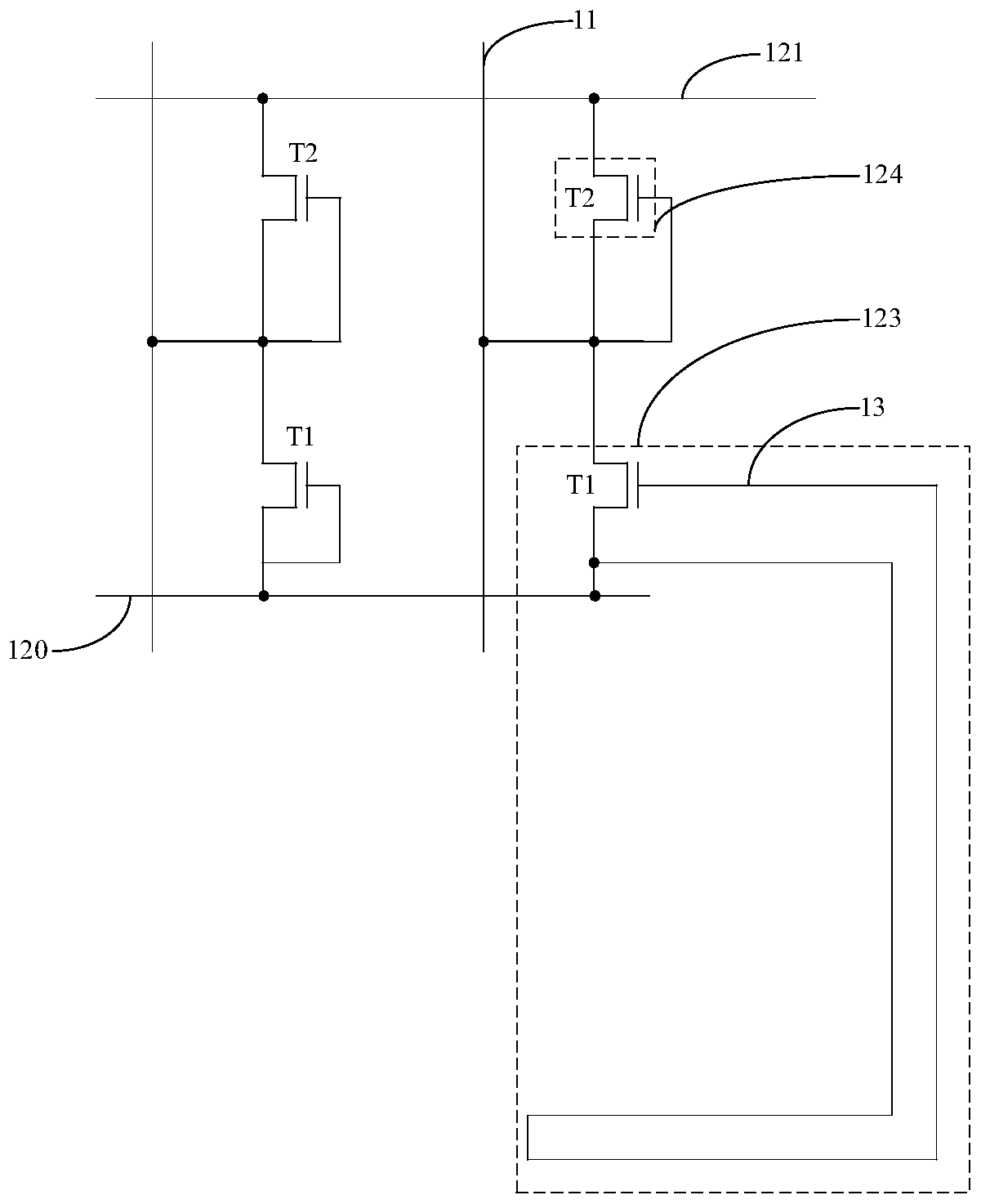
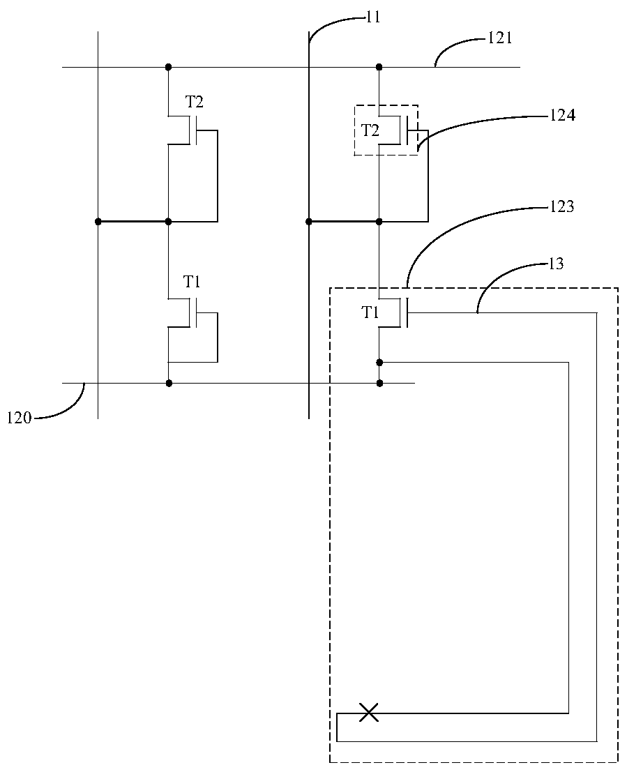
[0036] In the related art, when making an organic light emitting diode display, generally, a display motherboard is fabricated first, and then the display motherboard is cut to form a single display substrate. The single display substrate can also be called a cell unit. In order to ensure The reliability of the display substrate. After the display substrate is cut and formed, the display substrate will be tested for lighting. In addition to testing whether the display substrate can achieve normal display functions, the lighting test can also detect whether there are cracks in the edge area of ​​the display substrate.

[0037] More specifically, in order to perform crack detection, crack dete...


PUM


Abstract

The invention discloses a display substrate, a manufacturing method thereof, a crack detection method and a display device, relates to the technical field of display, and aims at solving the problemsthat an existing crack detection mode is complex in operation and wiring difficulty in an edge area of a display screen is easily increased. The display substrate comprises a pixel unit and a data signal line, wherein the data signal line is used for writing a data voltage signal into the pixel unit. The display substrate further comprises an electrostatic discharge circuit, and the electrostaticdischarge circuit comprises a first electrostatic discharge line and a second electrostatic discharge line; a first electrostatic discharge sub-circuit which is connected with the data signal line andthe first electrostatic discharge line, wherein a connecting line included in the first electrostatic discharge sub-circuit is reused as a crack detection line, and the crack detection line is located in a peripheral area, surrounding the display area, in the display substrate and extends along the edge of the display substrate. The first electrostatic discharge sub-circuit is used for conductingthe connection between the data signal line and the first electrostatic discharge line when the crack detection line is broken in a detection period. The display substrate provided by the invention is used for displaying.

Description

technical field [0001] The invention relates to the field of display technology, in particular to a display substrate and a manufacturing method thereof, a crack detection method, and a display device. Background technique [0002] With the continuous development of display technology, the application of organic light emitting diode display is more and more extensive. During the preparation process of the organic light emitting diode display, cracks are prone to occur in the edge area of ​​the display, and the cracks are easy to affect the reliability of the display. make an impact. In the prior art, in order to ensure the reliability of the manufactured display screen, crack detection lines and detection circuits are generally arranged in the edge area of ​​the display screen, and whether there is a crack in the edge area of ​​the display screen is determined through the cooperation of the detection circuit and the crack detection line. [0003] Although the above method c...

Claims


Application Information

Patent Timeline
Patent Type & Authority Applications(China)
IPC IPC(8): H01L23/544H01L23/60G09F9/33G01R31/28
Inventor 包征孙世成陈功辛燕霞胡红伟李雪萍吴奕昊徐鹏
Owner BOE TECH GRP CO LTD
Why Eureka
Try Eureka