


Quick Research
Generate reliable direction feasibility study reports for your R&D in just a few steps.

Technical Q&A
Discover and master advanced knowledge NOW. Basics, ideas, possibilities, all at once.

Find Solutions
As an expert in R&D theories, this can generate solutions to your technical problems instantly.

Evaluate Feasibility
Analyze your overall solution with one click, know your potential R&D risks in advance.

Monitor Landscape
Get weekly tech updates, stay abreast of the latest tech innovations and key insights.
Glass-based chip rewiring packaging structure and manufacturing method thereof
A technology of packaging structure and manufacturing method, applied in semiconductor/solid-state device manufacturing, electrical components, electrical solid-state devices, etc., can solve problems such as high cost, technical difficulty, and complicated process, achieve excellent electrical performance, avoid complex processes, The effect of simplifying the process
- Summary
- Abstract
- Description
- Claims
- Application Information
AI Technical Summary
Problems solved by technology
Method used
Image

Examples
Embodiment 1
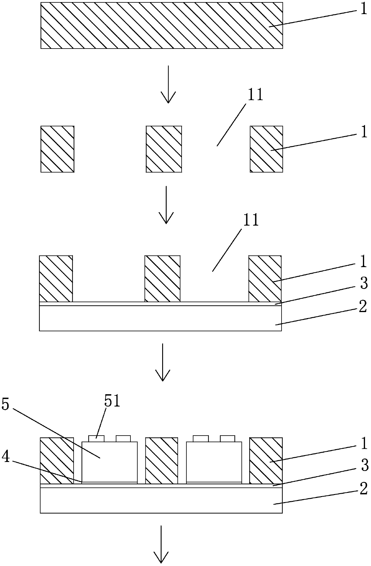
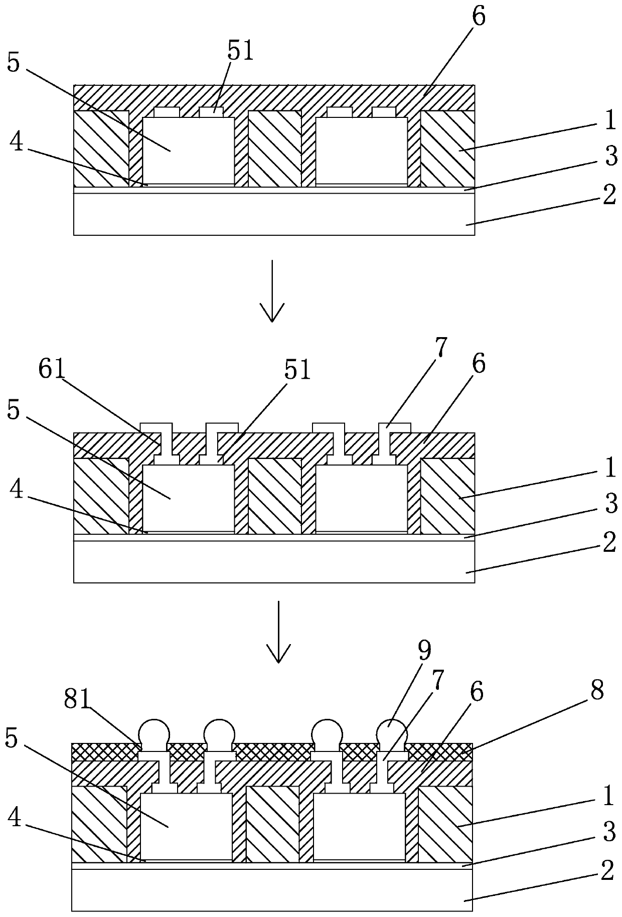
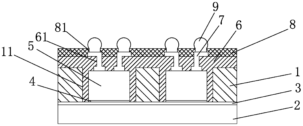
[0035] refer to figure 1 , a fabrication method of a glass-based chip rewiring package structure, corresponding to figure 1 Schematic diagram of the structure obtained in each step, the specific steps are:
[0036] 1) Provide a glass substrate 1, the thickness of the glass substrate 1 can be selected to be similar to the thickness of the chip to be packaged;
[0037] 2) Process the glass substrate 1 by laser or etching to form a through hole 11 penetrating up and down, and the size of the through hole 11 is slightly larger than the chip to be packaged;
[0038] 3) Adhering the lower surface of the glass substrate 1 to the carrier 2 through the first bonding layer 3, the carrier 2 can be a glass substrate, a silicon substrate or a ceramic substrate, etc.;
[0039] 4) Provide a chip 5 with a first pad 51, place the pad of the chip 5 facing up in the through hole 11, and the bottom surface of the chip 5 is adhered to the carrier plate 2 at the bottom of the through hole 11 thro...
Embodiment 2
[0046] refer to image 3 The difference between embodiment 2 and embodiment 1 is that the carrier plate 2' of this embodiment is obtained after the carrier plate 2 in embodiment 1 is thinned, and the overall thickness is reduced to meet the use requirements.
Embodiment 3
[0048] refer to Figure 4 , The difference between embodiment 3 and embodiment 1 is that the step of removing the carrier plate is also included, and the final structure obtained does not contain the carrier plate, which further reduces the thickness.
PUM
 Abstract
Description
Claims
Application Information
 - R&D Engineer
- R&D Manager
- IP Professional
- Industry Leading Data Capabilities
- Powerful AI technology
- Patent DNA Extraction
Browse by: Latest US Patents, China's latest patents, Technical Efficacy Thesaurus, Application Domain, Technology Topic, Popular Technical Reports.
© 2024 PatSnap. All rights reserved.Legal|Privacy policy|Modern Slavery Act Transparency Statement|Sitemap|About US| Contact US: help@patsnap.com