3d NAND memory and its formation method

A 3DNAND, memory technology, applied in the direction of semiconductor devices, electric solid state devices, electrical components, etc., can solve the problems of stack dislocation, wafer warping and sliding, high production cost, prevent dent defects, small thermal stress, high temperature deformation Effect

Active Publication Date: 2021-04-13
YANGTZE MEMORY TECH CO LTD
View PDF2 Cites 0 Cited by
  • Summary
  • Abstract
  • Description
  • Claims
  • Application Information

AI Technical Summary

Problems solved by technology

[0004] Among them, the Array Common Source (ACS for short) is an important structure requiring high conductivity. Currently, there are many schemes for forming the Array Common Source. In the first scheme, ACS is usually filled with tungsten (W). , although tungsten has good electrical conductivity, in the process of its formation, due to the large stress, it will cause various process problems, such as wafer warping and sliding, photolithography deformation, stacking dislocation, etc., which will lead to device performance degradation of
Therefore, in the second solution, polysilicon is used to replace tungsten, but the conductivity of polysilicon is much lower than that of tungsten. Even if doped polysilicon is used, its conductivity is still much lower than that of tungsten, and the production cost is relatively high.
[0005] The third solution takes both stress and resistance into account. This solution is to form a common source of the array by forming a polysilicon layer and a metal layer on the polysilicon layer. residual

Method used


Image

  • 3d NAND memory and its formation method
  • 3d NAND memory and its formation method
  • 3d NAND memory and its formation method

Examples


Embodiment Construction

[0048] As mentioned in the background art, conventionally, when forming a polysilicon layer and a metal layer on the polysilicon layer to form an array common source, residues of the metal layer are likely to occur.

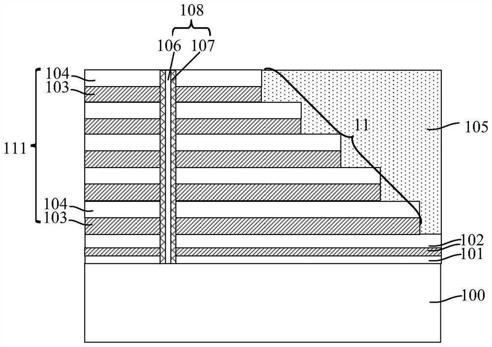
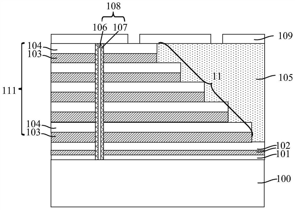
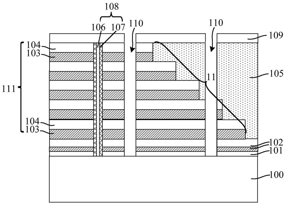
[0049] Research has found that the formation process of 3D NAND memory is as follows: firstly, a stack structure with alternately stacked sacrificial layers and isolation layers is formed on the semiconductor substrate, and the end of the stack structure has a stepped structure; a dielectric layer covering the stepped structure is formed; A plurality of gate spacers are formed in the stacked structure on one side of the stepped structure; a polysilicon material layer is formed on the stacked structure and the dielectric layer and in the gate spacers; a chemical mechanical polishing process removes the polysilicon on the stacked structure and the dielectric layer material layer, and then etch back to remove part of the thickness of the polysilicon material layer, f...


PUM


Abstract

A 3D NAND memory and its forming method, wherein the forming method includes forming a dielectric layer covering the stepped structure; forming a number of dummy vias in the dielectric layer and the stepped structure, and the dummy vias are filled with a dummy via material layer, the hardness of the pseudo-via material layer is greater than that of the dielectric layer; after the formation of the pseudo-via material layer, a number of grid isolation grooves are formed in the dielectric layer and the step structure; a conductive semiconductor is formed in the grid isolation grooves layer, the surface of the conductive semiconductor layer is lower than the surface of the dielectric layer; a metal layer is formed on the conductive semiconductor layer, and the metal layer fills the gate spacer. The method of the invention prevents the residue of the metal layer.

Description

technical field [0001] The invention relates to the field of semiconductor manufacturing, in particular to a 3D NAND memory and a forming method thereof. Background technique [0002] NAND flash memory is a better storage device than hard disk drives, and it has been widely used in electronic products as people pursue non-volatile storage products with low power consumption, light weight and high performance. At present, the planar NAND flash memory is close to the limit of practical expansion. In order to further increase the storage capacity and reduce the storage cost per bit, a 3D NAND memory is proposed. [0003] At present, the main components of 3D NAND memory can include array storage units and peripheral circuits, and the data access operations in each storage unit are realized through the control of peripheral circuits. Therefore, in the manufacturing process of 3D NAND memory, the conductance of each part Rate is an important link that cannot be ignored. [0004...

Claims


Application Information

Patent Timeline
Patent Type & Authority Patents(China)
IPC IPC(8): H01L27/115H01L27/11575H01L27/11582H01L27/1157
CPCH10B43/35H10B43/50H10B43/27
Inventor 汤召辉
Owner YANGTZE MEMORY TECH CO LTD
Why Eureka
Try Eureka