Active matrix substrate and method for manufacturing same
An active matrix and manufacturing method technology, applied in semiconductor/solid-state device manufacturing, light source, electric light source, etc., can solve problems such as difficult characteristics, and achieve the effect of suppressing the reduction of mass production and TFT characteristics
- Summary
- Abstract
- Description
- Claims
- Application Information
AI Technical Summary
Problems solved by technology
Method used
Image


Examples
no. 1 Embodiment approach
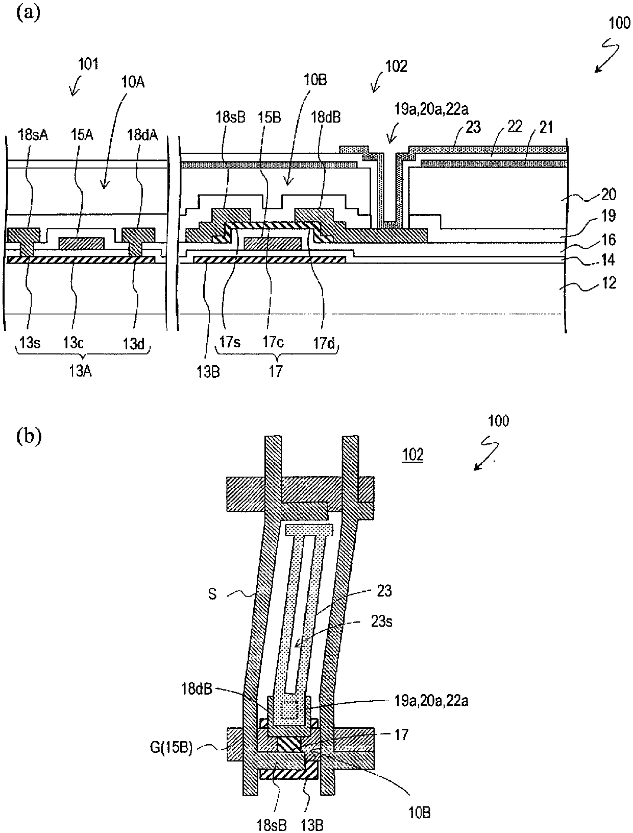
[0035] figure 1 (a) shows a schematic cross-sectional view of an active matrix substrate 100 (hereinafter referred to as "TFT substrate 100") according to the first embodiment of the present invention, figure 1 (b) shows a schematic plan view of a pixel region of the TFT substrate 100 . in addition, figure 2 A schematic top view of the entire TFT substrate 100 is shown.
[0036] Such as figure 2 As shown, the TFT substrate 100 has: a display area 102 including a plurality of pixels; and an area other than the display area 102 (non-display area). The non-display area includes a drive circuit formation area 101 where a drive circuit is provided. For example, a gate driver circuit 140 , a source driver circuit 150 , and an inspection circuit 170 are provided in the driver circuit formation region 101 .
[0037] A plurality of gate bus lines (not shown) extending in the row direction and a plurality of source bus lines S extending in the column direction are formed in the d...
no. 2 Embodiment approach
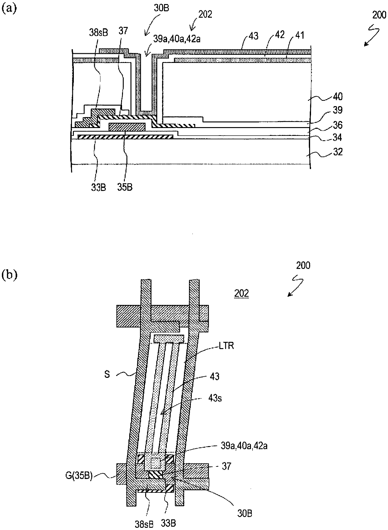
[0082] refer to image 3 (a) and image 3 (b) describes the structure of the TFT substrate 200 according to the second embodiment of the present invention. The structure of the second TFT 30B for pixels of the TFT substrate 200 is different from that of the TFT substrate 100 of the first embodiment. The other structures are the same as those of the TFT substrate 100, and thus descriptions thereof are omitted. In addition, the TFT substrate 200 can be easily manufactured only by changing the manufacturing method of the TFT substrate 100 .
[0083] image 3 (a) shows a schematic cross-sectional view of the second TFT 30B for pixels of the TFT substrate 200, image 3 (b) shows a schematic plan view of the pixel region of the TFT substrate 200 .
[0084] The TFT substrate 200 includes a substrate 32 and a second TFT 30B formed in a display region 202 on the substrate 32 . The driving circuit formation area (not shown) on the substrate 32 has figure 1 The first TFT10A is sh...
no. 3 Embodiment approach
[0088] Figure 4 (a) shows a schematic cross-sectional view of the second TFT 50B for a pixel of the TFT substrate 300, Figure 4 (b) shows a schematic plan view of a pixel region of the TFT substrate 300 .
[0089] The TFT substrate 300 includes a substrate 52 and a second TFT 50B formed in a display region 302 on the substrate 52 . The driver circuit forming region (not shown) on the substrate 52 has figure 1 The first TFT10A is shown.
[0090] The second TFT 50B is a bottom-gate TFT, and includes: a gate electrode 55B; a second insulating layer 36 covering the gate electrode 55B; and an oxide semiconductor layer 57 disposed on the second insulating layer 56 . Here, the gate electrode 55B is provided on the silicon semiconductor layer 53B formed on the substrate 52 and the first insulating layer 54 covering the silicon semiconductor layer 53B. Like the TFT substrate 100, the silicon semiconductor layer 53B is formed on the same level as the crystalline silicon semicondu...
PUM
| Property | Measurement | Unit |
|---|---|---|
| thickness | aaaaa | aaaaa |
| thickness | aaaaa | aaaaa |
| thickness | aaaaa | aaaaa |
Abstract
Description
Claims
Application Information
 - R&D
- Intellectual Property
- Life Sciences
- Materials
- Tech Scout
- Unparalleled Data Quality
- Higher Quality Content
- 60% Fewer Hallucinations
Browse by: Latest US Patents, China's latest patents, Technical Efficacy Thesaurus, Application Domain, Technology Topic, Popular Technical Reports.
© 2025 PatSnap. All rights reserved.Legal|Privacy policy|Modern Slavery Act Transparency Statement|Sitemap|About US| Contact US: help@patsnap.com