MOSFET and power conversion circuit
A technology of positive charge density and area, applied in circuits, output power conversion devices, electrical components, etc., can solve problems such as large changes in switching characteristics
- Summary
- Abstract
- Description
- Claims
- Application Information
AI Technical Summary
Problems solved by technology
Method used
Image

Examples
Embodiment approach 1
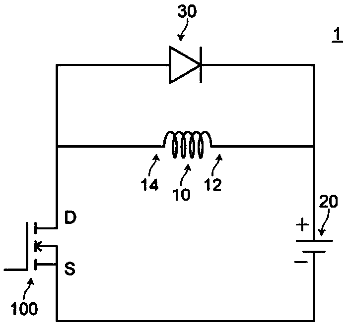
[0055] 1. Configuration and operation of the power conversion circuit 1 according to the first embodiment
[0056] The power conversion circuit 1 according to the first embodiment is a chopper circuit as a component such as a DC-DC converter or an inverter. The power conversion circuit 1 related to the first embodiment is as figure 1 As shown, it includes: a reactor 10 ; a power supply 20 ; a MOSFET 100 related to Embodiment 1; and a rectifying element 30 .
[0057] The reactor 10 is a passive element capable of storing energy in a magnetic field formed by passing an electric current.
[0058] The power source 20 is a DC power source that supplies current to the reactor 10 . MOSFET 100 controls the current supplied to reactor 10 by power supply 20 . Specifically, the MOSFET 100 performs switch switching in response to a clock signal applied to the gate electrode of the MOSFET 100 by a driving circuit (not shown), and once it is in a conductive state, conduction between the...
Embodiment approach 2
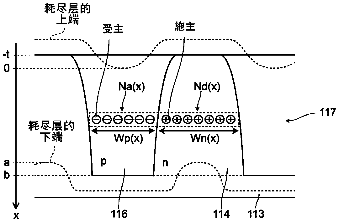
[0147] MOSFET 102 according to Embodiment 2 basically has the same configuration as MOSFET 100 according to Embodiment 1, but differs from MOSFET 100 according to Embodiment 1 in that it does not change the width at a predetermined depth position in the n-type columnar region. w n (x) and the width w at the specified depth position in the p-type columnar region p (x), but changes the positive charge density N d (x) and the density N of negative charges at a specified depth position in the p-type columnar region a (x). That is, in the MOSFET 102 according to Embodiment 2, as shown in FIG. 12 , the positive charge density N d (x) and the density N of negative charges at a specified depth position in the p-type columnar region 116 a When (x) is the vertical axis, the density N of the positive charge d (x) exhibits a convex monotonous upward curve to the right, and the density of the negative charge N a (x) exhibits a downwardly convex monotonous curve that droops to the rig...
Embodiment approach 3
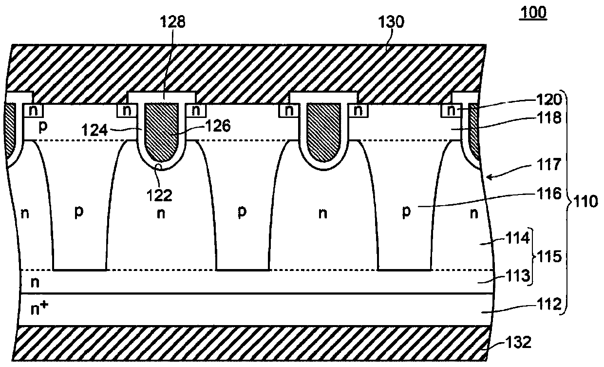
[0151] MOSFET 200 according to Embodiment 3 basically has the same configuration as MOSFET 100 according to Embodiment 1, but differs from MOSFET 100 according to Embodiment 1 in that it is a trench gate MOSFET rather than a planar gate MOSFET. That is, in the MOSFET 200 related to the third embodiment, the semiconductor substrate 210 is as Figure 13 As shown, it has: a base region 218 formed on the surface of the first main surface of the semiconductor substrate 210, and formed on the entire surface of the p-type columnar region 216 and a part of the surface of the n-type columnar region 214; formed on The surface of the first main surface of the semiconductor base 210, and the n-type surface high-concentration region 219 adjacent to the base region 218 formed on the surface of the n-type columnar region 214, and the surface of the base region 218 In the n-type source region 220, the gate electrode 236 is formed on the surface of the base region 218 sandwiched by the source ...
PUM
| Property | Measurement | Unit |
|---|---|---|
| Thickness | aaaaa | aaaaa |
| Thickness | aaaaa | aaaaa |
Abstract
Description
Claims
Application Information
 - R&D
- Intellectual Property
- Life Sciences
- Materials
- Tech Scout
- Unparalleled Data Quality
- Higher Quality Content
- 60% Fewer Hallucinations
Browse by: Latest US Patents, China's latest patents, Technical Efficacy Thesaurus, Application Domain, Technology Topic, Popular Technical Reports.
© 2025 PatSnap. All rights reserved.Legal|Privacy policy|Modern Slavery Act Transparency Statement|Sitemap|About US| Contact US: help@patsnap.com