Manufacturing method of light emitting device
A light-emitting device and a manufacturing method technology, which are applied to components of lighting devices, semiconductor devices of light-emitting elements, lighting devices, etc., and can solve problems such as inability to directly connect to AC mains, lower production efficiency, yield rate, and high manufacturing difficulty. , to achieve the effect of low processing difficulty, reduce the difficulty of stamping, and low cost
- Summary
- Abstract
- Description
- Claims
- Application Information
AI Technical Summary
Problems solved by technology
Method used
Image
Examples
Embodiment 1
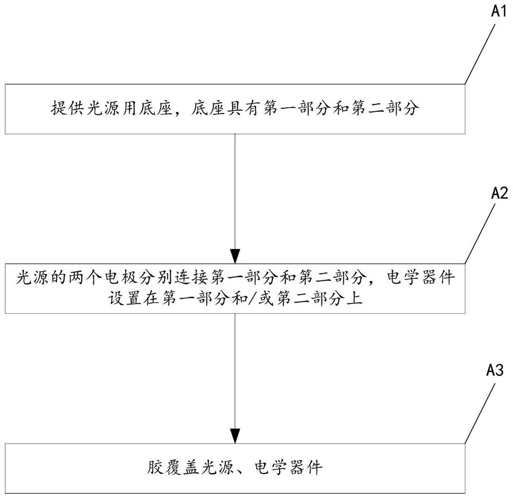
[0039] figure 1 A flow chart of the manufacturing method of the light-emitting device according to Embodiment 1 of the present invention is schematically given, as shown in figure 1 As shown, the manufacturing method of the light emitting device includes the following steps:
[0040] (A1) Obtain a base for a light source, the base has a first part and a second part that are isolated from each other, and the first part and the second part are connected by insulating plastic; the way to obtain the base for a light source is:
[0041] (B1) Provide a carrier, the carrier includes a strip-shaped conductor, and the strip-shaped conductor has a plurality of bearing units distributed in a matrix; the carrier includes:
[0042] A strip-shaped conductor, the strip-shaped conductor has a plurality of carrying units distributed in a matrix; the carrying unit includes:
[0043] The first part, one end of the first part that is away from the extending direction of the strip-shaped conduct...
Embodiment 2
[0076] An application example of the method for manufacturing a light emitting device according to Embodiment 1 of the present invention.
[0077] In the carrier of this application example, the strip-shaped conductor has carrying units distributed in a matrix; along the extending direction of the strip-shaped conductor, a third connecting portion is provided between adjacent first connecting portions, The width of the first connecting portion is greater than the width of the third connecting portion; the second connecting portion extends along the extending direction; in the extending direction, the first connecting portion and the third connecting portion are shared, such as the first connecting portion distributed sequentially The bearing unit, the second bearing unit and the third bearing unit, the second part of the first bearing unit and the first part of the second bearing unit share the first connection part, the second part of the second bearing unit and the first part...
Embodiment 3
[0091] An application example of the method for manufacturing a light emitting device according to Embodiment 1 of the present invention.
[0092] The difference with embodiment 2 is:
[0093] 1. There is a through hole at the connection part between the first connecting part and the first part, and the first (through) hole on the through hole and the first part both extends along a direction perpendicular to the extending direction of the strip conductor, and the through hole The length and the width of the hole are larger than the first (through) hole on the first part; part of the through hole is the same as the through hole;
[0094]2. There is a through hole in the third connecting part, the width of the through hole along the extending direction is greater than the width of the connecting part between the third connecting part and the second connecting part, the through hole and the second part The second (through) holes extend along a direction perpendicular to the ex...
PUM
 Abstract
Description
Claims
Application Information
 - Generate Ideas
- Intellectual Property
- Life Sciences
- Materials
- Tech Scout
- Unparalleled Data Quality
- Higher Quality Content
- 60% Fewer Hallucinations
Browse by: Latest US Patents, China's latest patents, Technical Efficacy Thesaurus, Application Domain, Technology Topic, Popular Technical Reports.
© 2025 PatSnap. All rights reserved.Legal|Privacy policy|Modern Slavery Act Transparency Statement|Sitemap|About US| Contact US: help@patsnap.com

