
Electroplating equipment for improving PCB high-aspect-ratio hole-filling capacity and copper plating uniformity

A PCB board with high thickness-to-diameter ratio technology, which is applied in the field of electroplating equipment to improve the ability of filling holes with high thickness-to-diameter ratio of PCB boards and the uniformity of copper plating. It can solve the problems of uneven surface copper thickness, high cost, and uneven hole copper thickness. To achieve the effect of increasing uniform fluidity, improving longitudinal fluidity, and ensuring penetration ability

Active Publication Date: 2019-04-05
黄湘琪
View PDF5 Cites 11 Cited by
  • Summary
  • Abstract
  • Description
  • Claims
  • Application Information

AI Technical Summary

Problems solved by technology

In the existing technology, the ordinary gantry electroplating line can no longer meet the requirements of high aspect ratio printed circuit board electroplating, and then use the pulse electroplating line, such as reducing the current and prolonging the electroplating time, still can not solve the liquid medicine in the dead corner of the electroplating tank Fluidity problem; switch plating parameters by using a large number of dummy plates with accompanying plating when switching between different material numbers, but it will also lead to poor plating results: such as uneven copper thickness in holes, uneven copper thickness on the surface, and high and slightly Difficult PCB boards with high aspect ratios cannot meet the requirements at all. At the same time, a large number of dummy boards are used to switch plating parameters, which will cause various problems such as low production efficiency and high cost.
[0003] In the existing technology, the traditional electroplating tank production equipment can no longer meet the requirements of high aspect ratio printed circuit board electroplating, mainly in the uneven thickness of copper in the hole (thick copper at the hole, thin hole in the middle of the hole), which not only brings There is a kneeling problem in the component plug-in, and there is a radiation problem during high-speed signal transmission;

Method used


Image

  • Electroplating equipment for improving PCB high-aspect-ratio hole-filling capacity and copper plating uniformity
  • Electroplating equipment for improving PCB high-aspect-ratio hole-filling capacity and copper plating uniformity
  • Electroplating equipment for improving PCB high-aspect-ratio hole-filling capacity and copper plating uniformity

Examples


Embodiment Construction

[0032] Specific embodiments of the present invention will be described in detail below in conjunction with the accompanying drawings.

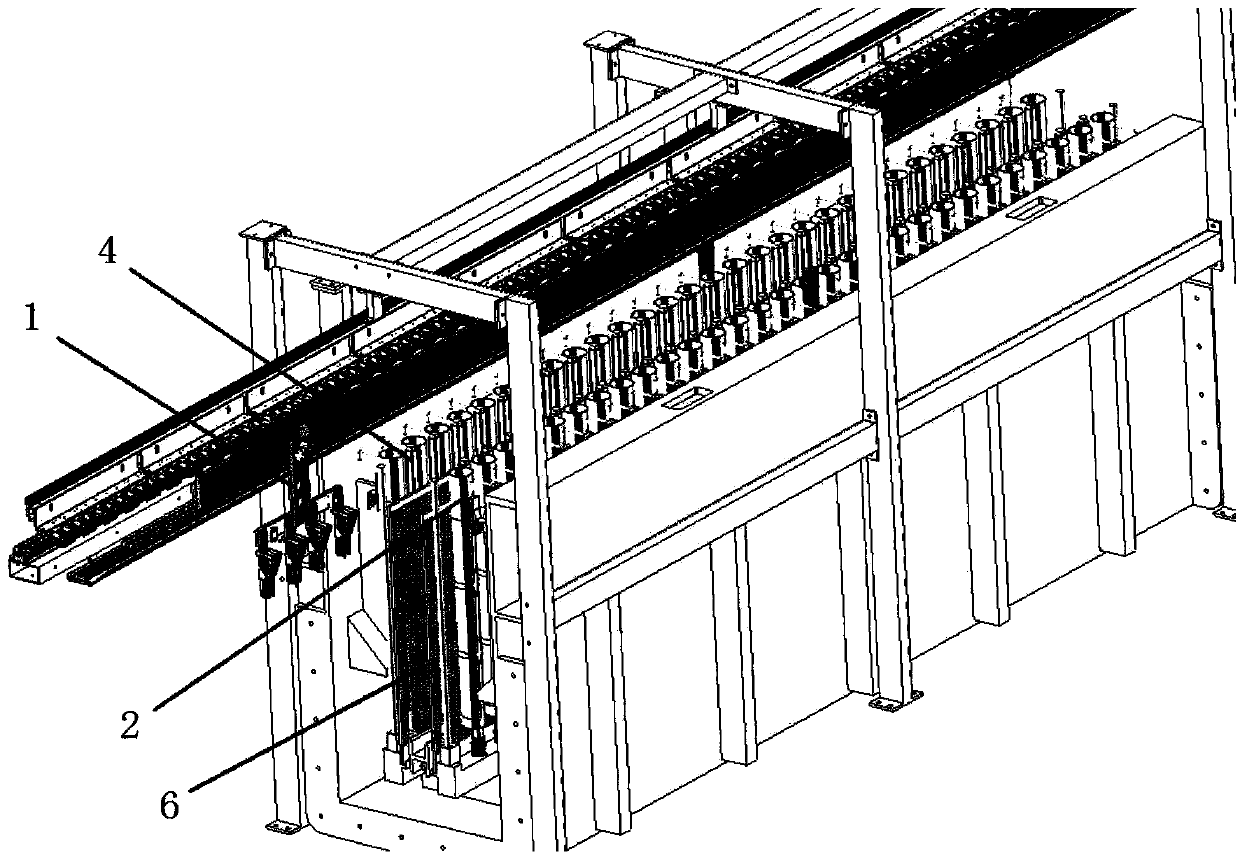
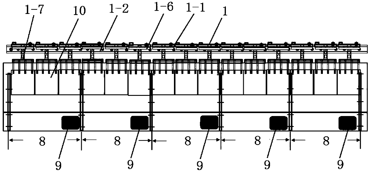
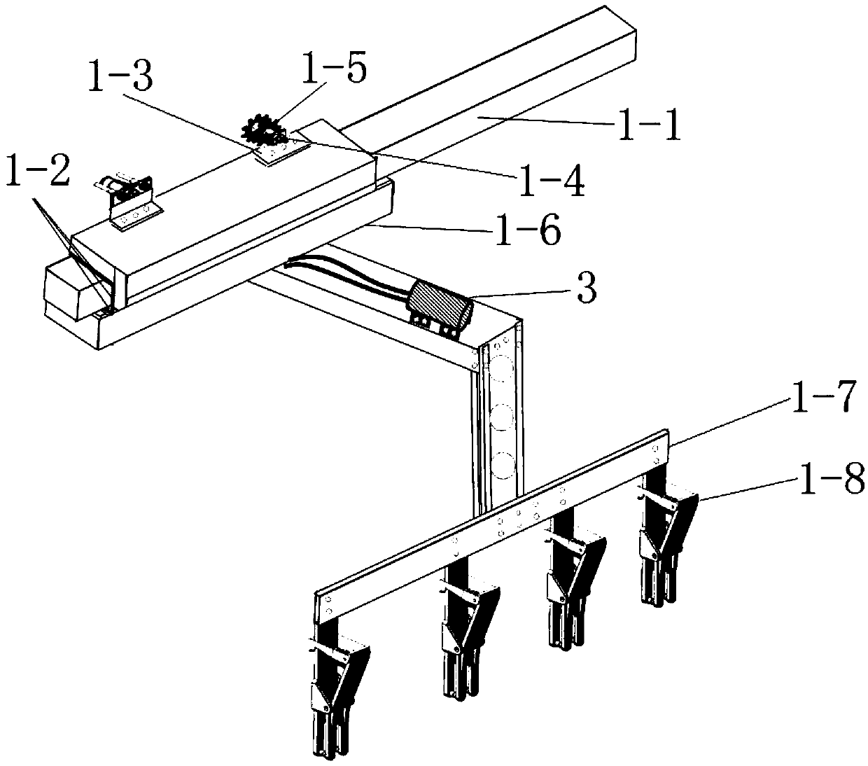
[0033] Such as Figure 1-Figure 7 As shown, the electroplating equipment for improving the high-thickness-diameter ratio filling capacity of PCB boards and the uniformity of copper plating in the embodiment of the present invention is composed of a specially designed tank body for anti-inductance, and the core of the tank body design includes (the special method for improving the tank liquid filling capacity) Arranged spray pipes and nozzles, high-uniformity anode power line baffles, jet tubes for lifting bath circulation and stirring, electroplating fixtures equipped with vibration motors), anti-inductance pulse power supplies, anti-inductance cables and other core parts composition;

[0034] Specifically, the present invention includes: a transmission flyer 1, an electroplated titanium basket 2, a vibrating device 3, a nozzle 4, a jet pipe ...


PUM


Abstract

The invention discloses electroplating equipment for improving the PCB high-aspect-ratio hole-filling capacity and copper plating uniformity so as to improve the hole-filling capacity during high-aspect-ratio PCB electroplating. The equipment comprises an electroplating bath, a transmission feiba part which is disposed over the electroplating bath, electroplating titanium baskets, spaying pipes and processing solution tank bases, wherein the electroplating titanium baskets, the spaying pipes and the processing solution tank bases are arranged in the electroplating bath; spray nozzles are disposed on the spraying pipes; the electroplating titanium baskets and the spraying pipes are divided into two groups and are arranged in the electroplating bath; the processing solution tank bases are arranged corresponding to the two groups of electroplating titanium baskets and spraying pipes; anode baffles are disposed on the opposite sides of the two groups of spraying pipes correspondingly; andthe spray nozzles are located in leakage holes formed in the anode baffles. During electroplating, a to-be-electroplated PCB is located between the anode baffles, and then the spray nozzles face the to-be-electroplated PCB.

Description

technical field [0001] The invention belongs to the technical field of electroplating, and more specifically relates to an electroplating device for improving the ability of filling holes with a high thickness-to-diameter ratio of a PCB board and the uniformity of copper plating. Background technique [0002] In recent years, with the rapid development of the electronics industry, the requirements for printed circuit boards (referred to as PCB boards) are getting higher and higher. High board thickness-to-aperture ratio (the ratio of board thickness to aperture ≥ 12:1) PCB Boards have become mainstream in design. The key to electroplating of high-aspect-ratio PCBs lies in the electroplating of through-holes. The key to electroplating through-holes lies in the improvement of the ability of the electroplating solution to penetrate the through-holes and the uniformity of copper thickness. In the existing technology, the ordinary gantry electroplating line can no longer meet th...

Claims


Application Information

Patent Timeline
Patent Type & Authority Applications(China)
IPC IPC(8): C25D17/00C25D5/08C25D5/02C25D7/00
CPCC25D5/02C25D5/08C25D7/00C25D17/00
Inventor 黄安琪黄奥琪黄佑琪黄云钟陈翠曹磊磊黄云雷黄丹丹
Owner 黄湘琪
Learn More