
Chip packaging structure, chip packaging method, and display device

A packaging structure and chip packaging technology, applied in semiconductor/solid-state device components, semiconductor devices, electrical components, etc., can solve problems such as chip and circuit board hole phenomenon, chip packaging reliability reduction, etc., to improve production efficiency, fill The effect of improving efficiency and reducing resistance

Active Publication Date: 2019-03-29
BOE TECH GRP CO LTD +1
View PDF9 Cites 2 Cited by
  • Summary
  • Abstract
  • Description
  • Claims
  • Application Information

AI Technical Summary

Problems solved by technology

[0004] The purpose of the present invention is to provide a chip packaging structure, packaging method, and display device, which are used to solve the problem that holes are easily generated between the chip and the circuit board after the bottom filling operation when the chip is packaged, causing the chip to be damaged. The problem of reduced reliability of the package

Method used


Image

  • Chip packaging structure, chip packaging method, and display device
  • Chip packaging structure, chip packaging method, and display device
  • Chip packaging structure, chip packaging method, and display device

Examples


Embodiment Construction

[0068] In order to further illustrate the chip packaging structure, packaging method, and display device provided by the embodiments of the present invention, a detailed description will be given below in conjunction with the accompanying drawings.

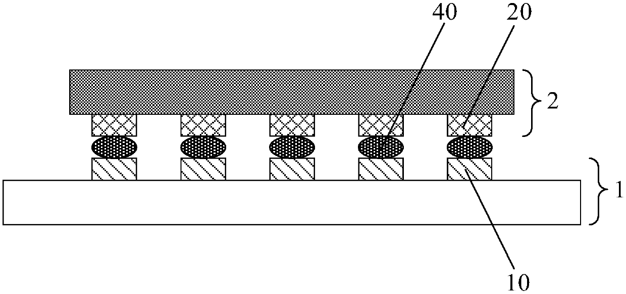
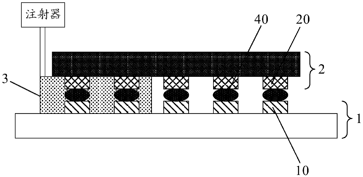
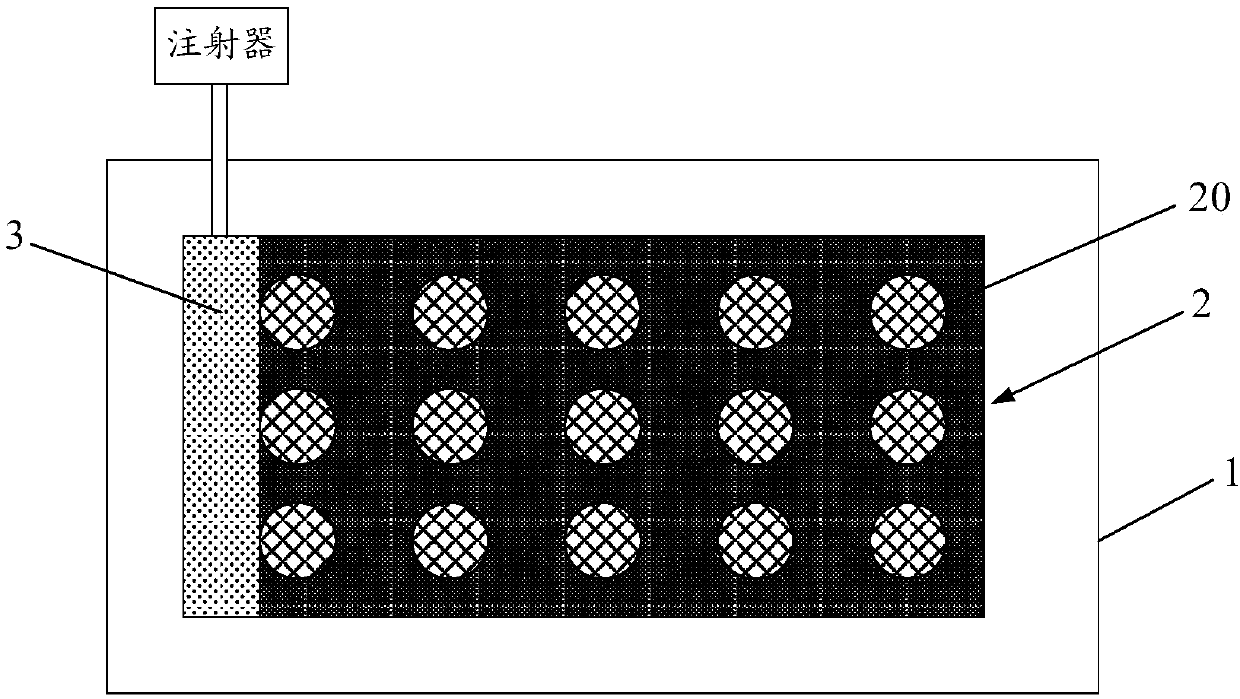
[0069] like figure 1 As shown, when the chip 2 is packaged on the circuit board 1, the chip 2 is generally packaged on the chip package area on the circuit board 1, and the chip package area includes pads corresponding to the pins 20 in the chip 2 one-to-one. 10. When packaging, first deposit solder balls 40 on the pins 20 of the chip 2, and then place the side of the chip 2 with the pins 20 facing the circuit board 1, so that each pin 20 in the chip 2 is connected to the circuit board 1. Contact the corresponding pad 10, and then heat the solder ball 40 between the pin 20 and the pad 10, so as to realize the electrical connection between the pin 20 and the corresponding pad 10; as figure 2 and image 3 As shown, the underfill ...


PUM


Abstract

The invention discloses a chip packaging structure, a chip packaging method and a display device, relates to the technical field of packaging, and aims to solve the problem that when a chip is packaged, a hole phenomenon is easily generated between the chip and a circuit board after bottom filling operation is carried out, so that the chip packaging reliability is reduced. The chip packaging structure comprises a circuit board, a chip arranged in a chip packaging area and a filling material filled between the chip and the circuit board, wherein the chip comprises a plurality of pins which arein one-to-one correspondence with a plurality of bonding pads on the circuit board, and the pins are electrically connected with the corresponding bonding pads to form conductive parts. The circuit board is corresponding disposed in the region of a gap between the adjacent conductive parts, and at least a part of the region is provided with a first groove; and / or at least a part of the area, corresponding to the gap between the adjacent conductive parts, of the chip is provided with a second groove. The chip packaging structure provided by the invention is used for providing a driving signal.

Description

technical field [0001] The present invention relates to the field of packaging technology, in particular to a chip packaging structure, packaging method, and display device. Background technique [0002] The flip-chip packaging process is a packaging method in which solder balls are deposited on the pins of the flip-chip, then the flip-chip is turned over and heated, and the flip-chip is combined with the circuit board using the molten solder balls. When using this packaging method to package the chip, after the chip is combined with the circuit board, the filling material will be used to fill the bottom between the chip and the circuit board. The main purpose of the bottom filling is to increase the size of the chip and the circuit board. The contact area between the chip and the circuit board is improved, the thermal stress between the chip and the circuit board is released, and the solder ball is protected. [0003] However, as the transmission capability of the chip inc...

Claims


Application Information

Patent Timeline
Patent Type & Authority Applications(China)
IPC IPC(8): H01L23/13H01L23/31H01L21/56
CPCH01L21/56H01L23/13H01L23/3157H01L2224/16225H01L2224/32225H01L2224/73204H01L2224/83385H01L2224/92125H01L2924/00
Inventor 李伟王静王莉
Owner BOE TECH GRP CO LTD
Learn More