
Method for fabricating OLED display panel and OLED display panel

A display panel and manufacturing method technology, applied in semiconductor/solid-state device manufacturing, organic semiconductor devices, electrical components, etc., can solve the problems of lack of photoresist, affecting the performance of display devices, changes in metal surfaces, etc., to ensure stable quality sexual effect

Inactive Publication Date: 2019-03-26
WUHAN CHINA STAR OPTOELECTRONICS SEMICON DISPLAY TECH CO LTD
View PDF4 Cites 3 Cited by
  • Summary
  • Abstract
  • Description
  • Claims
  • Application Information

AI Technical Summary

Problems solved by technology

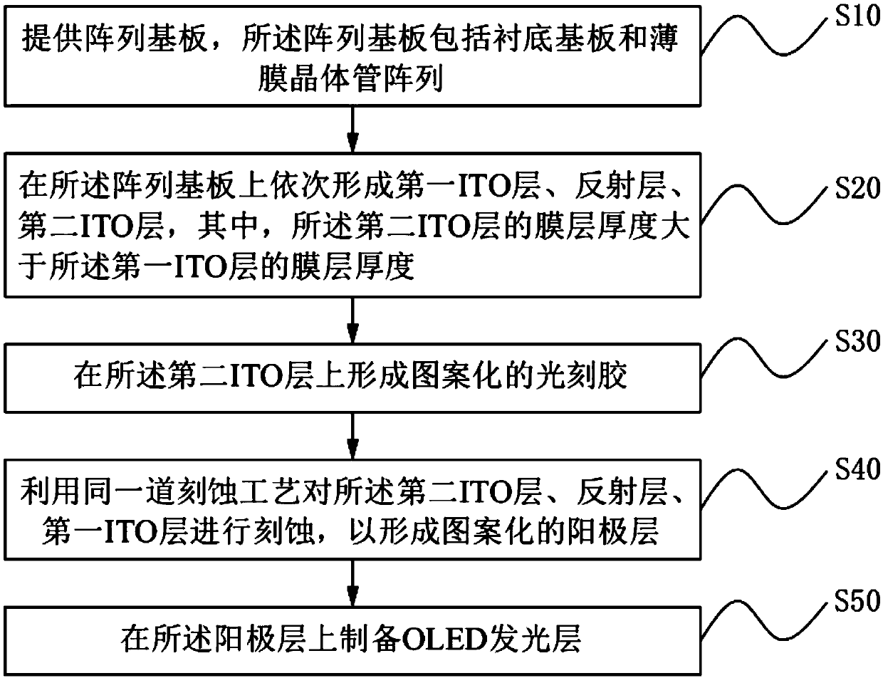
[0004] The present invention provides a method for manufacturing an OLED display panel to solve the problem that in the existing OLED manufacturing method, since the photoresist may be missing during the etching process when preparing the OLED anode, the metal layer does not need to be etched Exposed, resulting in changes in the metal surface, which in turn affects the technical problems of the performance of the display device

Method used


Image

  • Method for fabricating OLED display panel and OLED display panel
  • Method for fabricating OLED display panel and OLED display panel
  • Method for fabricating OLED display panel and OLED display panel

Examples


Embodiment Construction

[0032] The description of the following embodiments refers to the attached drawings to illustrate specific embodiments in which the present invention can be implemented. The directional terms mentioned in the present invention, such as [Up], [Down], [Front], [Back], [Left], [Right], [Inner], [Outer], [Side], etc., are for reference only The direction of the additional schema. Therefore, the directional terms used are used to describe and understand the present invention, rather than to limit the present invention. In the figure, units with similar structures are indicated by the same reference numerals.

[0033] The present invention is directed to the existing manufacturing method of the OLED display panel. Since the photoresist may be missing during the etching process when the OLED anode is prepared, the areas where the metal layer does not need to be etched are exposed, resulting in changes in the properties of the metal surface. Furthermore, the technical problem that affe...


PUM


Abstract

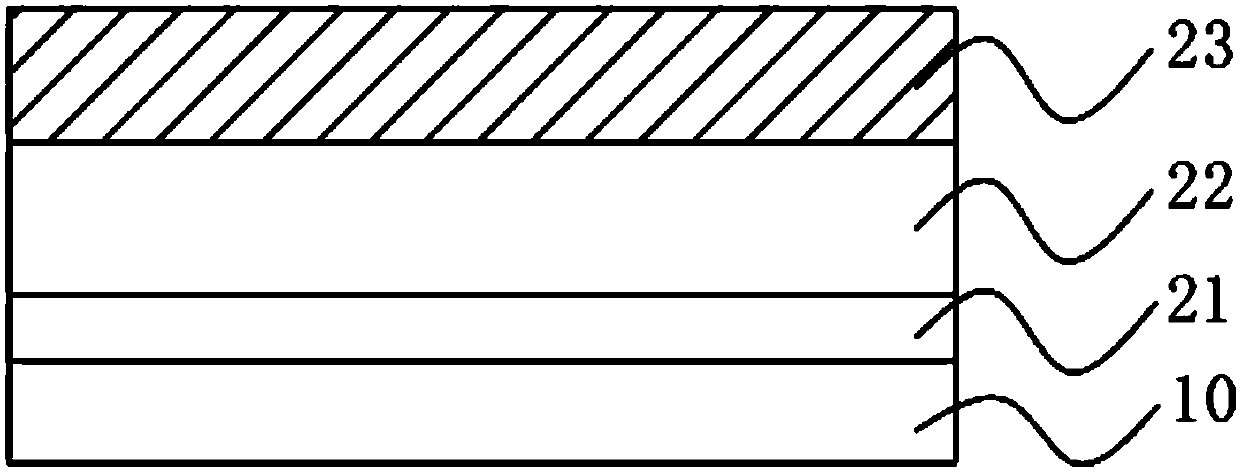
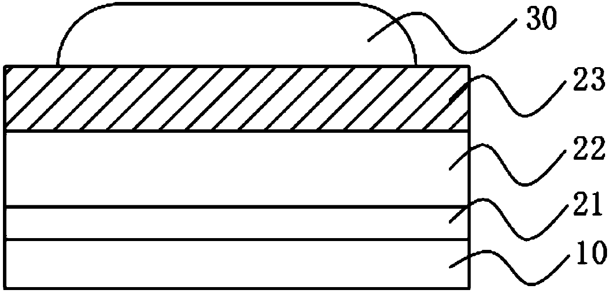
A method for fabricating an OLED display panel comprises providing an array substrate including a base substrate and a thin film transistor array; forming a first ITO layer, a reflective layer, and asecond ITO layer on the array substrate, wherein the thickness of the second ITO layer is greater than the thickness of the first ITO layer; forming a patterned photoresist on the second ITO layer; etching the second ITO layer, the reflective layer, and the first ITO layer by the same etching process to form a patterned anode layer; and preparing an OLED light-emitting layer on the anode layer. The method prolongs the etching time of the top ITO film layer by increasing the thickness of the top ITO film layer, thereby avoiding influences on the metal surface at the lower layer caused by the absence of the photoresist during the etching process and ensuring the quality stability of products.

Description

Technical field [0001] The present invention relates to the field of display technology, in particular to a manufacturing method of an OLED display panel and an OLED display panel. Background technique [0002] OLED (Organic Light-Emitting Diode, organic light-emitting diode) display technology has the advantages of self-luminescence, wide viewing angle, high contrast, low power consumption, and high response speed, and has become the object of research in the field of optoelectronics. According to the light extraction method, OLED displays can be divided into top-emission type and bottom-emission type. For traditional bottom-emission type OLED devices, the light needs to pass through the bottom array substrate to emit light. The metal devices on the array substrate will block part of the light. The problem of low aperture ratio: The light of the top-emission OLED device does not need to pass through the substrate, and is emitted from above the OLED light-emitting layer, avoiding...

Claims


Application Information

Patent Timeline
Patent Type & Authority Applications(China)
IPC IPC(8): H01L51/56H01L51/52H10K99/00
CPCH10K71/00H10K59/80515H10K59/80518H10K71/621H10K59/1201H10K2102/351H10K85/50H10K50/818H10K50/813H10K59/12H10K2102/103
Inventor 李镇石
Owner WUHAN CHINA STAR OPTOELECTRONICS SEMICON DISPLAY TECH CO LTD
Learn More