
Self-powered semiconductor photocatalytic devices with WSA position-sensitive structure

A photoelectric catalysis and semiconductor technology, applied in semiconductor devices, electrical components, chemical instruments and methods, etc., can solve the problem of energy consumption, complex structure of photoelectric catalytic devices, and catalytic purification effect of semiconductor photoelectric catalytic devices not always in the best state, etc. question

Active Publication Date: 2021-10-01
CHANGCHUN UNIV OF SCI & TECH +1
View PDF6 Cites 0 Cited by
  • Summary
  • Abstract
  • Description
  • Claims
  • Application Information

AI Technical Summary

Problems solved by technology

However, to make a thin film photoanode, an external power supply provides a bias voltage, which complicates the structure of the photocatalytic device and requires additional energy consumption. In addition, the catalytic area of ​​the catalytic material in the thin film state is limited, and it is easy to deactivate.
[0004] There is still a technical problem in the existing technology. When semiconductor photocatalytic devices are used for catalytic purification of natural water bodies, the light source for photocatalysis is sunlight, and as time passes from morning to night, the intensity and angle of sunlight are changing. The catalytic purification effect of semiconductor photocatalytic devices is not always in the best state

Method used


Image

  • Self-powered semiconductor photocatalytic devices with WSA position-sensitive structure
  • Self-powered semiconductor photocatalytic devices with WSA position-sensitive structure
  • Self-powered semiconductor photocatalytic devices with WSA position-sensitive structure

Examples


Embodiment Construction

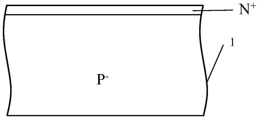
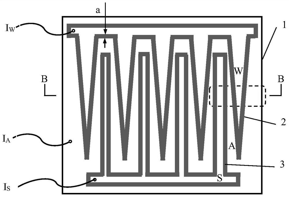
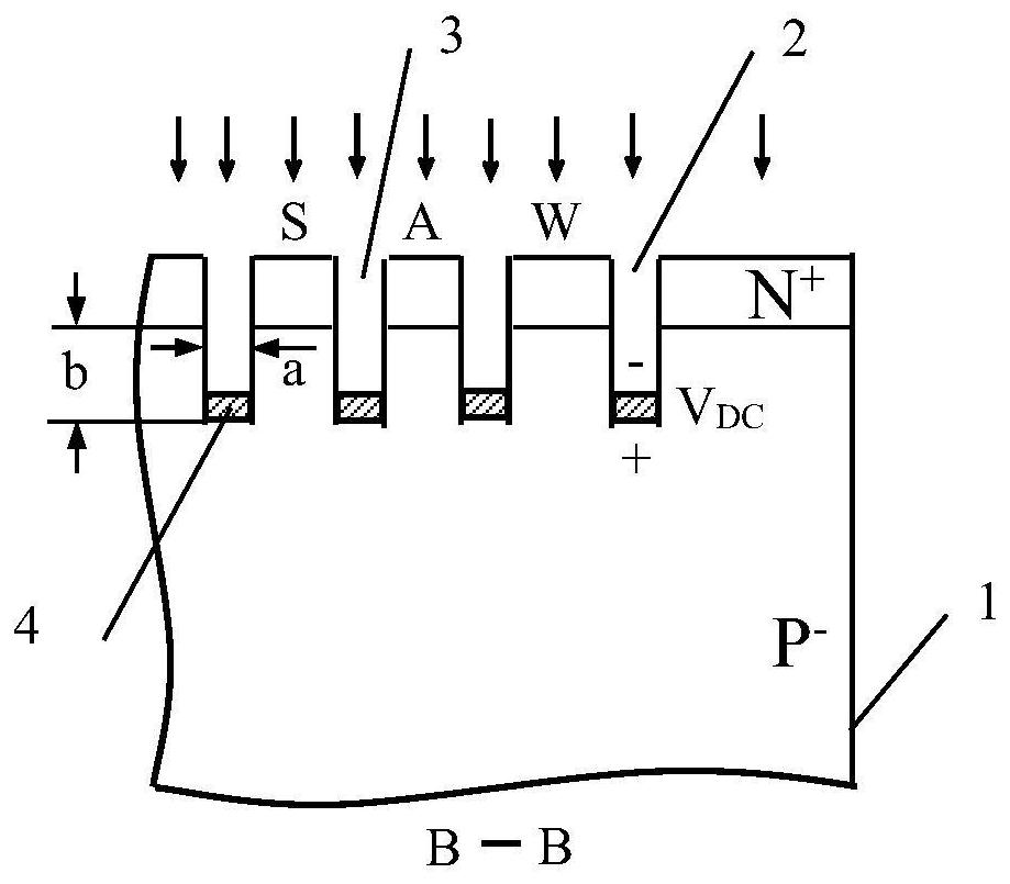
[0010] Self-powered semiconductor photocatalytic device with WSA position-sensitive structure of the present invention such as Figure 1 ~ Figure 3 As shown, at P - N + N of Wafer 1 + A set of wedge-shaped anodes W and a set of strip-shaped anodes S, P are distributed across the surface of the zone - N + Silicon wafer 1 thick 600μm, N + The thickness of the area is 20 μm, the part between the wedge-shaped anode W and the strip-shaped anode S is the third anode A, the wedge-shaped anode W, the strip-shaped anode S, and the third anode A are separated by the wedge-shaped anode channel 2 and the strip-shaped anode channel 3; The channel width a of the wedge-shaped anode channel 2 and the strip-shaped anode channel 3 is 100-120 μm, such as 100 μm, and the bottom of the channel is located at P - area, the channel is located at P - The depth b of the zone part is 50-120 μm, such as 120 μm, and a semiconductor nanowire photocatalytic layer 4 is distributed at the bottom of the c...


PUM

PropertyMeasurementUnit
thicknessaaaaaaaaaa
widthaaaaaaaaaa
thicknessaaaaaaaaaa

Abstract

A self-powered semiconductor photocatalytic device with a WSA position-sensitive structure belongs to the technical field of photoelectric catalysis. Existing semiconductor photoelectrocatalytic devices cannot keep their catalytic purification effect always in the best state during the passage of sunshine time. The present invention is characterized in that, at P ‑ N + N of silicon wafer + A group of wedge-shaped anodes W and a group of strip-shaped anodes S are distributed across the surface of the area. The part between the wedge-shaped anode W and the strip-shaped anode S is the third anode A. The wedge-shaped anode W, the strip-shaped anode S, and the third anode A are composed of wedge-shaped The anode channel and strip-shaped anode channel are separated; the channel width a of the wedge-shaped anode channel and the strip-shaped anode channel is 100-120 μm, and the bottom of the channel is located at P ‑ area, the channel is located at P ‑ The depth b of the zone part is 50-120 μm, and the semiconductor nanowire photocatalytic layer is distributed at the bottom of the channel, and the thickness of the semiconductor nanowire photocatalytic layer is 1-2 μm; P ‑ District to N + The doping concentration of the region changes from lean to rich. The invention can make use of the WSA position-sensitive structure to make the semiconductor photocatalytic device track sunlight and ensure the amount of light energy received.

Description

technical field [0001] The invention relates to a self-powered semiconductor photoelectric catalytic device with a WSA position-sensitive structure, which can be used to catalyze and purify water bodies, realize self-power supply by using light, and improve catalytic efficiency. Anode) enables the semiconductor photocatalytic device to track sunlight to ensure light energy reception, and belongs to the field of photocatalytic technology. Background technique [0002] Semiconductor photocatalytic technology began with TiO, which came out in 1972 2 (Titanium dioxide) catalyzes the purification of sewage. The technology incorporates TiO 2 The thin film acts as an electrode, and the photolysis of water occurs under the condition of light, so as to play a catalytic role. Later, semiconductor energy band theory was used to explain TiO 2 Photocatalytic mechanism, when the incident photon energy is greater than that of TiO 2 When the semiconductor band gap is wide, the electron...

Claims


Application Information

Patent Timeline
Patent Type & Authority Patents(China)
IPC IPC(8): H01L31/00C02F1/30C02F1/46
CPCC02F1/30C02F1/46C02F2201/002C02F2305/10
Inventor 母一宁陈卫军杨继凯曹喆肖楠王帅刘春阳
Owner CHANGCHUN UNIV OF SCI & TECH
Learn More