
Self-driven heterojunction infrared photodetector based on two-dimensional palladium diselenide nano-film and germanium and preparation method thereof

A technology of electrical detectors and palladium nanometers, which is applied in the field of photoelectric detection, can solve problems that are difficult to realize, and achieve the effects of low cost, high specific detection rate, and high responsivity

Active Publication Date: 2019-03-12
HENAN HANWEI ELECTRONICS
View PDF3 Cites 8 Cited by
  • Summary
  • Abstract
  • Description
  • Claims
  • Application Information

AI Technical Summary

Problems solved by technology

Third, the strong light-matter interaction of 2D materials offers the possibility to design miniaturized infrared photodetectors, which are difficult to achieve in conventional bulk semiconductor-based infrared photodetectors.

Method used


Image

  • Self-driven heterojunction infrared photodetector based on two-dimensional palladium diselenide nano-film and germanium and preparation method thereof
  • Self-driven heterojunction infrared photodetector based on two-dimensional palladium diselenide nano-film and germanium and preparation method thereof
  • Self-driven heterojunction infrared photodetector based on two-dimensional palladium diselenide nano-film and germanium and preparation method thereof

Examples


Embodiment 1

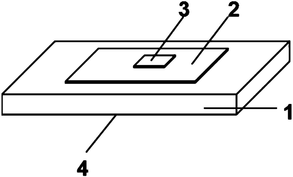
[0031] see figure 1 , the present embodiment is based on a self-driven heterojunction infrared photodetector of two-dimensional palladium diselenide nano-film and germanium, which has the following structure: a two-dimensional palladium diselenide nano-film 2 is tiled on the upper surface of a germanium substrate 1 On the two-dimensional palladium diselenide nano-film 2, the first metal electrode 3 that is in ohmic contact with the two-dimensional palladium diselenide nano-film 2 is provided, and the lower surface of the germanium substrate 1 is provided with a germanium substrate 1 that is in ohmic contact The second metal electrode 4;

[0032] A heterojunction is formed between the germanium substrate 1 and the two-dimensional palladium diselenide nano-film 2, and the first metal electrode 3 and the second metal electrode 4 are used as two output stages to construct a self-driven heterojunction infrared photodetector

[0033] The preparation method of the heterojunction inf...


PUM

PropertyMeasurementUnit
electrical resistivityaaaaaaaaaa
thicknessaaaaaaaaaa
thicknessaaaaaaaaaa

Abstract

The invention discloses a self-driven heterojunction infrared photodetector based on a two-dimensional palladium diselenide nano-film and germanium and a preparation method thereof. The two-dimensional palladium diselenide nano-film is deposited on the surface of a germanium substrate; metal electrodes in ohmic contact with the two-dimensional palladium diselenide nano-film and the germanium substrate are arranged on the two-dimensional palladium diselenide nano-film and the germanium substrate; the palladium diselenide and the germanium form a heterojunction, and the two metal electrodes serve as two output stages, so that the self-driven heterojunction infrared photodetector is constructed. The self-driven heterojunction infrared photodetector disclosed by the invention has simple preparation process, which realizes a wide response wave band, high responsivity, high detection rate and fast response speed at room temperature, and provides a way for designing a high-performance wide-band infrared detector.

Description

technical field [0001] The invention relates to a self-driven heterojunction infrared photodetector constructed by two-dimensional palladium diselenide nano film and germanium and a preparation method thereof, belonging to the technical field of photoelectric detection. Background technique [0002] A photodetector is a device that converts a received light signal into an electrical signal. Photoelectric detectors are widely used in various fields of military and national economy. In the infrared band, they are mainly used in industrial automatic control, missile guidance, infrared thermal imaging, infrared remote sensing, etc. [0003] Infrared photodetectors can be divided into many types according to different classification standards. The common classifications are: (1) According to the different physical mechanisms of detection, they can be divided into two categories: photon detectors based on various photoelectric effects and those realized by temperature changes. (2...

Claims


Application Information

Patent Timeline
Patent Type & Authority Applications(China)
IPC IPC(8): H01L31/105H01L31/0272H01L31/032H01L31/18
CPCH01L31/0272H01L31/032H01L31/105H01L31/1876Y02P70/50
Inventor 吴翟王媛鸽吴恩平贾诚史志锋李新建
Owner HENAN HANWEI ELECTRONICS
Learn More