Realization and Design Method of a Local Light Field Structure

A design method and light field technology, applied in the field of micro-nano photonics, can solve problems such as miss and long cycle, and achieve the effect of easy processing and time saving

Active Publication Date: 2020-06-05
BEIJING INSTITUTE OF TECHNOLOGYGY
View PDF0 Cites 0 Cited by
  • Summary
  • Abstract
  • Description
  • Claims
  • Application Information

AI Technical Summary

Problems solved by technology

However, these optical microcavity structures are all designed based on the photonic crystal structure. The periodic disorder is introduced into the photonic crystal structure by artificially designing defect positions or transfer matrices. It takes a lot of time to try the structure shape and parameters. Adjust to finally determine the structure with better effect, and the cycle of this process is quite long, and it has a lot of randomness, and it is possible to miss other structures that produce similar functions

Method used


Image

  • Realization and Design Method of a Local Light Field Structure
  • Realization and Design Method of a Local Light Field Structure
  • Realization and Design Method of a Local Light Field Structure

Examples


Embodiment 1

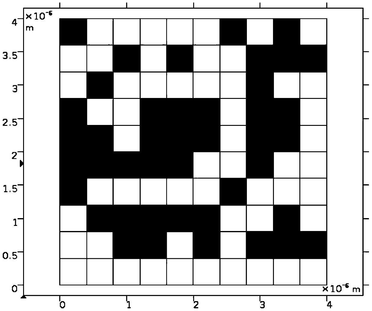
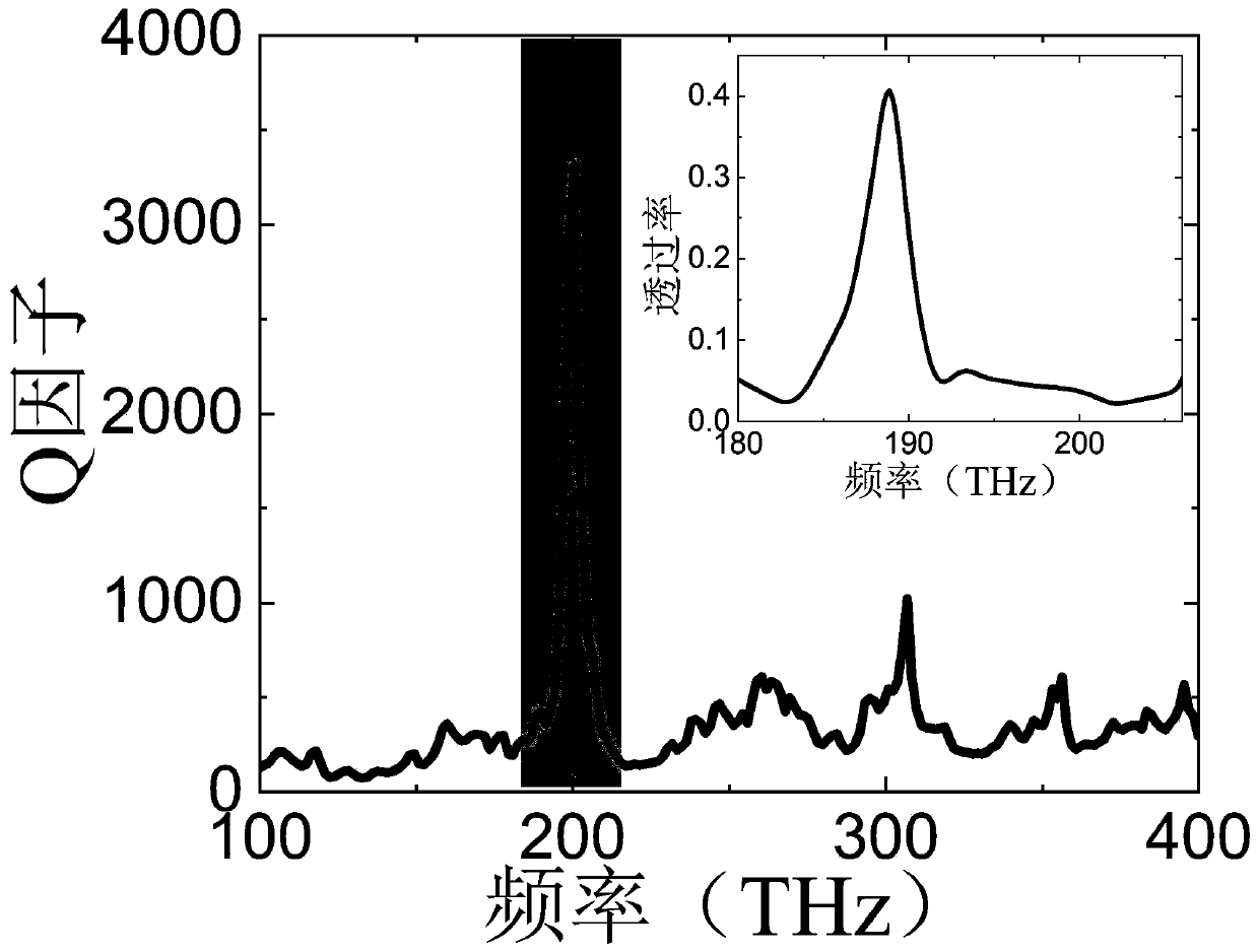
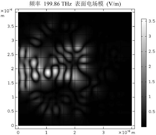
[0024] In order to verify the performance of the structural localized light field designed by the design method, a square localized light field structure with a side length of 4 μm was designed and divided into 10×10 square grids with a side length of 400 nm, and silicon and air were selected as materials. When the device is working, the linearly polarized light with a wavelength of 1500nm and perpendicular to the plane where the structure is located is incident from the central area of ​​the left edge of the structure.

[0025] This embodiment discloses a realization and design method of a local light field structure. A geometric model is preliminarily established in COMSOLMultiphysics, and the rectangular array function is used to realize the division of square grids. The filling material of each grid can only be silicon or air. "1" represents silicon, "0" represents air, and a random combination of "0" and "1" matrix is ​​used to represent the corresponding local light field...


PUM


Abstract

The invention discloses an implementation and design method of a local light field structure, and relates to the field of micro-nano photonics. The method comprises the steps that a plane of a to-be-designed area is subjected to grid division, the number of grids and the shape of each grid are determined, materials filling all the grids are represented by 0 and 1 matrices, a structure with the maximum optical quality factor (Q) is selected as a final result by means of an optimization algorithm, and the planar local light field structure with the highest Q is formed. By means of the method, the shape limitation is small, various structural parameters do not need to be separately optimized, the design process is directly completed by the algorithm, a lot of time can be saved, the shape is not limited by previous experience, and therefore the structure with the better effect can be generated. Since the planar structure easy to process is adopted, the local light field structure can be prepared by means of a micro-nano processing method and suitable for integrated application on chips, and the development of field related to local light fields is promoted.

Description

technical field [0001] The invention relates to the field of micro-nano photonics, in particular to a method for realizing and designing a localized light field structure. Background technique [0002] Light field localization can trap photons within a certain period of time, enhance the interaction between light and matter, and realize slow light effect, all-optical storage, optical sensing, etc. It is an emerging photonics technology. The localization of the light field has many physical properties, such as the spontaneous emission suppression behavior of light, energy transfer properties, etc., which makes the localized light field structure attract extensive attention in many research fields such as fundamental physics and applied photonics. At present, the main structure of localized light field is optical microcavity. An optical microcavity is a micro-nano-scale cavity structure in which light waves can be reflected back and forth to form resonance. The optical quali...

Claims


Application Information

Patent Timeline
Patent Type & Authority Patents(China)
IPC IPC(8): G02B27/00
CPCG02B27/0012
Inventor 路翠翠肖致远刘舟慧王慧琴刘晓宏
Owner BEIJING INSTITUTE OF TECHNOLOGYGY
Why Eureka
Try Eureka