Method and device for detecting patterned substrates
A technology for detecting patterns and substrates. It is used in transmittance measurement, scattering characteristic measurement, etc. It can solve the problems of bowl-shaped unevenness, inability to reflect local quality deviation, and large quality difference.
- Summary
- Abstract
- Description
- Claims
- Application Information
AI Technical Summary
Problems solved by technology
Method used
Image
Examples
Embodiment 1
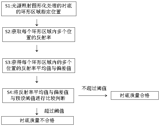
[0033] This embodiment provides the following method for detecting a patterned substrate, including the following steps:
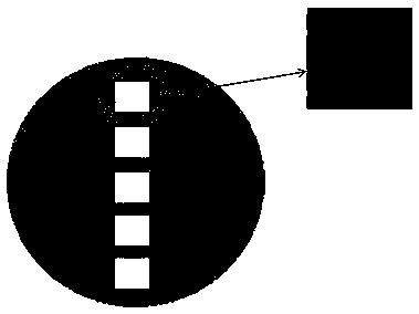
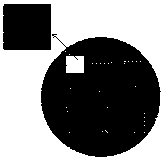
[0034] S1: Define the patterned surface of the substrate to be analyzed as a plurality of independently separated annular regions from the center to the edge;
[0035] The patterned substrate to be tested is a light-transmitting substrate, specifically the graphics on the surface of a sapphire substrate, and the current size is generally 2 inches (about 50mm in diameter), 4 inches (about 100mm in diameter) or 6 inches (about 150mm in diameter). ) of the sapphire substrate. The pattern on the surface of the sapphire substrate is obtained by dry or wet etching, and the pattern is cone, trapezoid, etc.;
[0036] The patterned substrate to be measured is a transparent insulating layer pattern, a DBR pattern, or an antireflection film pattern on the surface of a sapphire substrate, wherein the transparent insulating layer, DBR or antireflection film can be metal...
Embodiment 2
[0056] In order to implement the method described in Embodiment 1, this embodiment provides the following device for detecting a patterned substrate, such as Figure 5 As shown, the following components are included:
[0057] A light source 1, located on one side of the substrate 4, is used to irradiate a light beam to the substrate 4 to be tested for patterning, and the light beam is reflected or transmitted on the substrate to be tested for patterning; the irradiation It is direct irradiation or indirect irradiation, the light beam is a parallel light beam, and is hardly absorbed by the substrate and graphic material, and the light source with high light transmittance, the light source can be laser, single-color light source or white light, through the filter Or polarizers or optical lenses, as shown in the figure, are processed to obtain a single radiation direction or a single color beam, which is irradiated into the annular area.
[0058] An optical measuring instrument ...
PUM
 Abstract
Description
Claims
Application Information
 - Generate Ideas
- Intellectual Property
- Life Sciences
- Materials
- Tech Scout
- Unparalleled Data Quality
- Higher Quality Content
- 60% Fewer Hallucinations
Browse by: Latest US Patents, China's latest patents, Technical Efficacy Thesaurus, Application Domain, Technology Topic, Popular Technical Reports.
© 2025 PatSnap. All rights reserved.Legal|Privacy policy|Modern Slavery Act Transparency Statement|Sitemap|About US| Contact US: help@patsnap.com


