An organic light emitting display panel and a display device

A light-emitting display and organic technology, applied in semiconductor devices, electrical components, circuits, etc., can solve problems such as OLED device packaging failure

Active Publication Date: 2021-05-14
WUHAN TIANMA MICRO ELECTRONICS CO LTD
View PDF6 Cites 1 Cited by
  • Summary
  • Abstract
  • Description
  • Claims
  • Application Information

AI Technical Summary

Problems solved by technology

However, existing OLED devices often suffer from encapsulation failures

Method used


Image

  • An organic light emitting display panel and a display device
  • An organic light emitting display panel and a display device
  • An organic light emitting display panel and a display device

Examples


Embodiment Construction

[0028] The following will clearly and completely describe the technical solutions in the embodiments of the present invention with reference to the accompanying drawings in the embodiments of the present invention. Obviously, the described embodiments are only some, not all, embodiments of the present invention. Based on the embodiments of the present invention, all other embodiments obtained by persons of ordinary skill in the art without making creative efforts belong to the protection scope of the present invention.

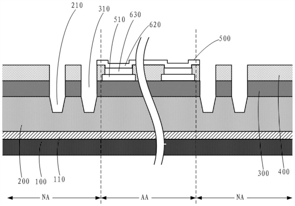
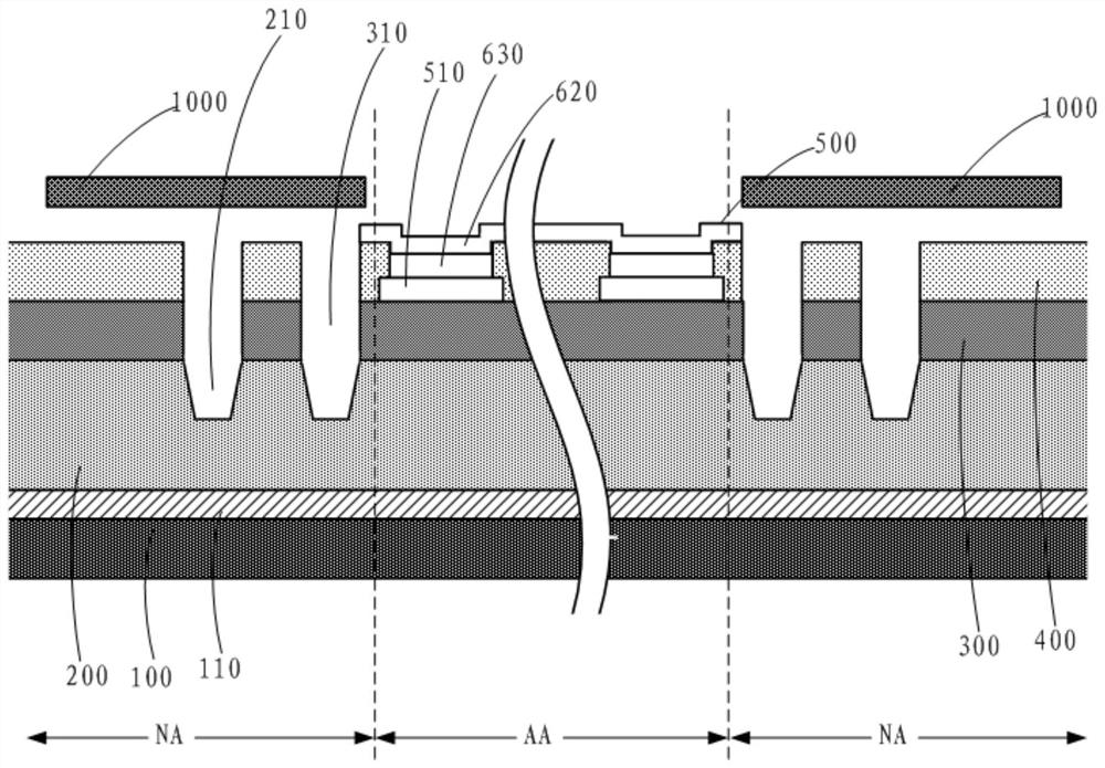
[0029] As mentioned in the background technology, as a self-illuminating display device, OLED devices do not require a separate light source, therefore, OLED devices can be driven at low voltage, and are easier to manufacture in a thinner and lighter shape; in addition, OLED devices have a wide viewing angle and high contrast ratio. And sensitive response speed and other advantages, so OLED devices are widely used in a variety of fields, such as smart mobile te...


PUM

PropertyMeasurementUnit
depthaaaaaaaaaa

Abstract

The present disclosure provides an organic light-emitting display panel and a display device, in which a plurality of depressions are arranged at the non-display area of ​​the transistor array layer, and the distance between the depressions and the edge close to the display area is 50 μm-500 μm, and, in the flat Form the hollowed out area exposing the sunken place corresponding to the hollowed out layer and the pixel definition layer, so as to reduce the surface height of the transistor array layer in this area through the setting of the sunken area, and remove the flattened layer and the pixel defined layer in this area by setting the hollowed out area The material of the area is used to avoid the situation that the mask plate scratches the surface of the transistor array layer corresponding to the depression and scratches the surface of the pixel definition layer corresponding to the hollow area during the subsequent production of the film layer structure, and improves the organic light-emitting display panel due to scratches. The failure of the encapsulation film layer.

Description

technical field [0001] The present invention relates to the technical field of organic light emitting display, and more specifically, relates to an organic light emitting display panel and a display device. Background technique [0002] Organic light-emitting display (Organic Light-Emitting Diode, OLED)) device is a self-luminous display device, OLED device includes a plurality of organic light-emitting devices, each organic light-emitting device includes an anode, a cathode, and an organic light-emitting layer between the anode and the cathode . Among them, the electron injection and hole injection to the organic light-emitting layer are realized through the cathode and the anode respectively, and the holes and electrons are recombined in the organic light-emitting layer to generate excitons, and these excitons transition from the excited state to the ground state, thereby generating light. [0003] As a self-luminous display device, OLED devices do not require a separate ...

Claims


Application Information

Patent Timeline
Patent Type & Authority Patents(China)
IPC IPC(8): H01L27/32
CPCH10K59/1213H10K59/122
Inventor 张国峰
Owner WUHAN TIANMA MICRO ELECTRONICS CO LTD
Why Eureka
Try Eureka