AMOLED display panel

A display panel and substrate substrate technology, applied in the direction of instruments, electrical digital data processing, electrical components, etc., can solve the problems that the front fingerprint affects the screen-to-body ratio, the rear fingerprint is inconvenient, and the screen-to-body ratio is limited, etc., to achieve Reduce space, realize full-screen design, and increase the effect of proportion

Inactive Publication Date: 2019-02-01
WUHAN CHINA STAR OPTOELECTRONICS SEMICON DISPLAY TECH CO LTD
View PDF7 Cites 7 Cited by
  • Summary
  • Abstract
  • Description
  • Claims
  • Application Information

AI Technical Summary

Problems solved by technology

These two kinds of fingerprint recognition have certain shortcomings. The front fingerprint affects the proportion of the screen, and the rear fingerprint is not very convenient.
[0003] figure 1 It is a common fingerprint identification design at present, a front fingerprint identification integrated in the home button, the fingerprint identification unit and the display area are independent of each other, and the fingerprint identification is placed in the lower area of ​​the display screen, which limits the screen-to-body ratio

Method used


Image

  • AMOLED display panel
  • AMOLED display panel
  • AMOLED display panel

Examples


Embodiment Construction

[0033] The following will clearly and completely describe the technical solutions in the embodiments of the present invention with reference to the drawings in the embodiments of the present invention. Apparently, the described embodiments are only some of the embodiments of the present invention, but not all of them. Based on the embodiments of the present invention, all other embodiments obtained by those skilled in the art without creative efforts fall within the protection scope of the present invention.

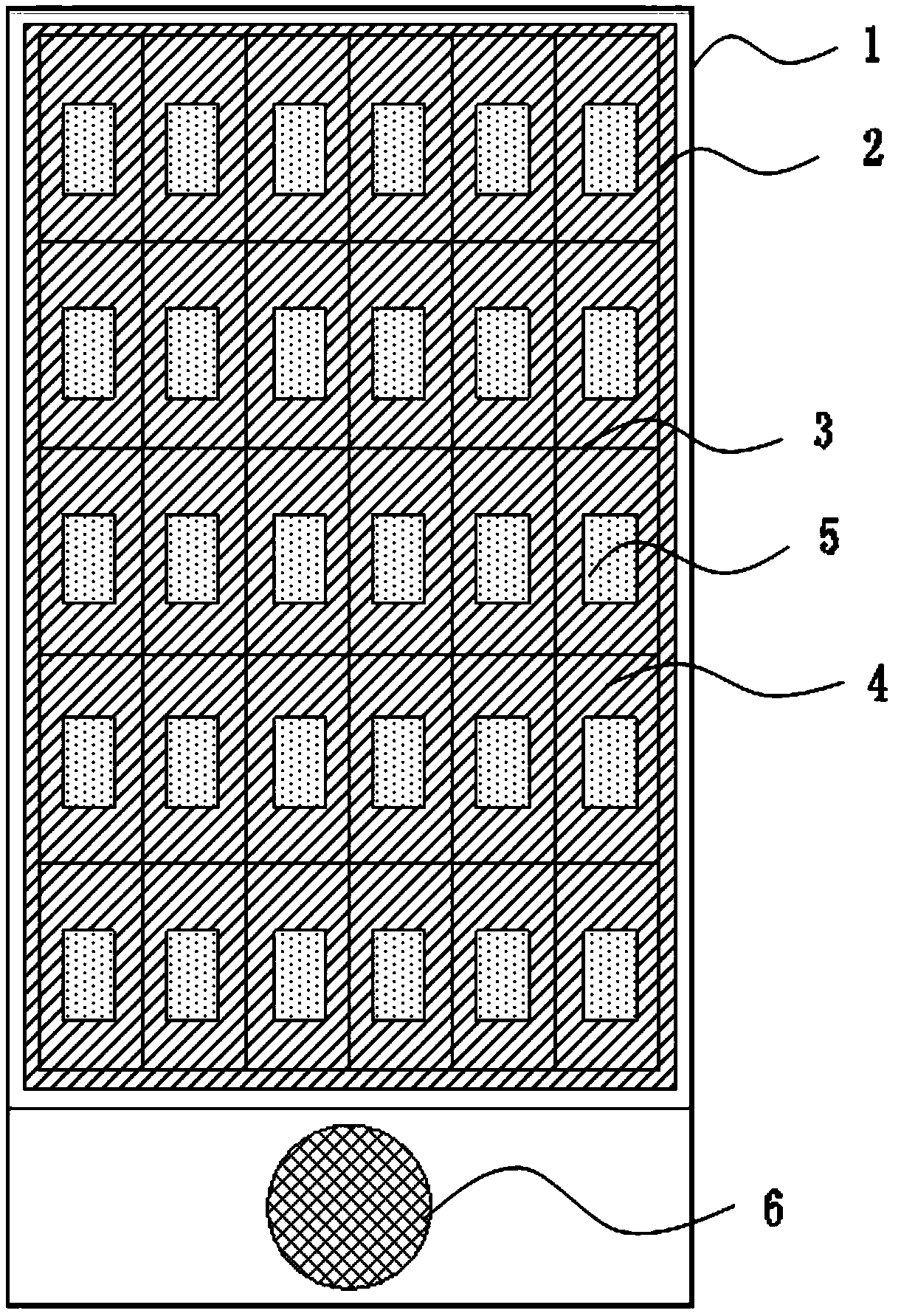
[0034] The present invention is aimed at the fingerprint identification design of the prior art. The fingerprint identification unit and the display area are independent of each other, and there is a technical problem of limiting the screen ratio. This embodiment can solve this defect.

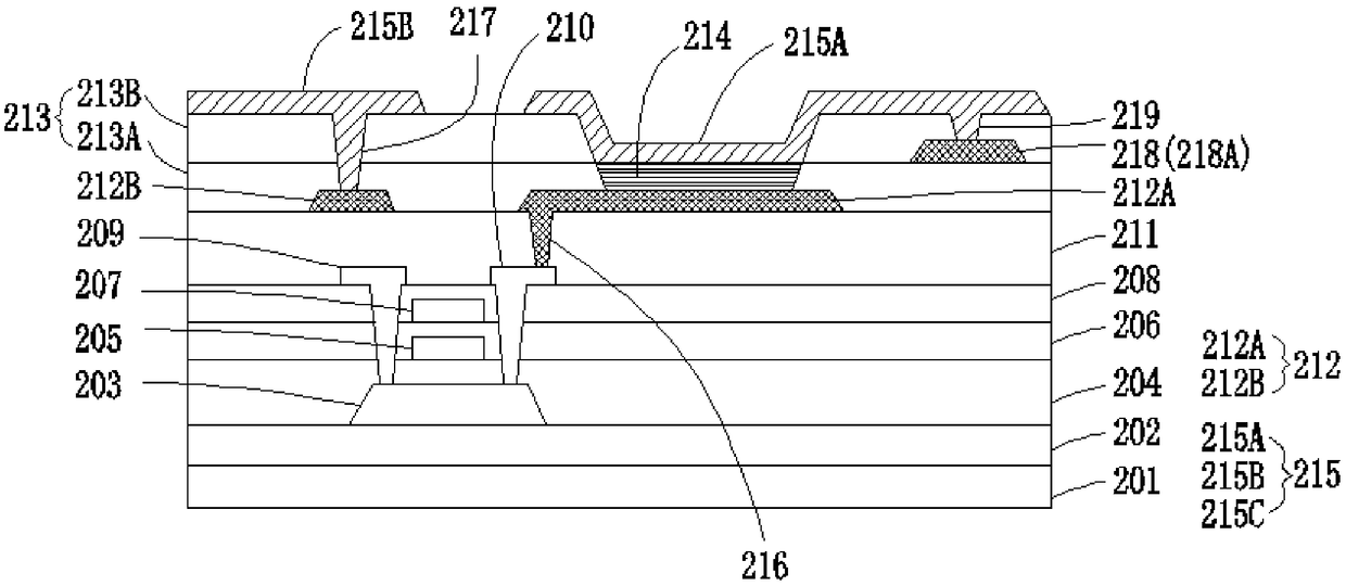
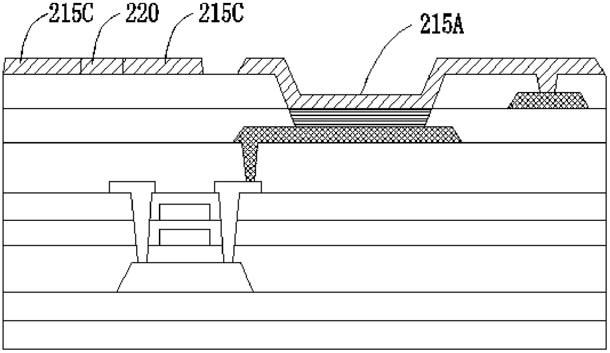
[0035] refer to Figure 2A , Figure 2A A schematic diagram of the film layer structure of the AMOLED display panel along the direction of the first electrode chain provided by the emb...


PUM


Abstract

The invention provides an AMOLED display panel which comprises a substrate, an anode layer arranged on the substrate, a pixel definition layer and a light emission layer arranged on the anode layer, asecond metal layer arranged on the pixel definition layer, and a cathode layer arranged on the pixel definition layer and the second metal layer. The cathode layer comprises cathodes arranged on thelight emission layer and induction electrodes electrically insulated from the cathodes, the induction electrodes form first electrode chain and second electrode chains insulated from the first electrode chains, the first and second electrode chains are independent from one another and distributed in an interlaced way, and the induction electrode in one first electrode chain and the induction electrode in the corresponding second electrode chain form a capacitor to realize fingerprint identification.

Description

technical field [0001] The present invention relates to the field of display technology, in particular to an AMOLED display panel. Background technique [0002] Active-matrix organic light emitting diode, referred to as AMOLED, is an active matrix organic light emitting diode panel. At present, there are two types of fingerprint identification solutions on the market. The first is the front fingerprint identification integrated in the home button, and the other is the rear fingerprint identification in the separate fingerprint identification area on the back of the fuselage. These two kinds of fingerprint recognition have certain shortcomings. The front fingerprint affects the proportion of the screen, and the rear fingerprint is not very convenient. [0003] figure 1 It is a common fingerprint identification design at present. It is a front fingerprint identification integrated in the home button. The fingerprint identification unit and the display area are independent of...

Claims


Application Information

Patent Timeline
Patent Type & Authority Applications(China)
IPC IPC(8): H01L27/32H01L51/52G06K9/00
CPCG06V40/1306H10K59/40H10K59/131H10K50/82G06F3/0446G06F3/0412G06F2203/04111G06V40/1318H10K59/1315H10K50/816H10K50/822H10K59/122
Inventor 郑园严志成
Owner WUHAN CHINA STAR OPTOELECTRONICS SEMICON DISPLAY TECH CO LTD
Why Eureka
Try Eureka