
Tiled photon neural network convolution layer chip

A neural network and convolution layer technology, which is applied in the field of intelligent photonic signal processing technology and neural network, can solve the problems of inability to accelerate neural network and large demand for deep learning calculation, and achieve the effect of low energy consumption and high energy consumption ratio

Active Publication Date: 2019-01-22
SHANGHAI JIAO TONG UNIV
View PDF6 Cites 11 Cited by
  • Summary
  • Abstract
  • Description
  • Claims
  • Application Information

AI Technical Summary

Problems solved by technology

Traditional deep learning is implemented by programming a computer in a central processing unit (hereinafter referred to as CPU) or a graphics processing unit (hereinafter referred to as GPU). For specialized applications, it is impossible to effectively specialize the acceleration of the neural network

Method used


Image

  • Tiled photon neural network convolution layer chip
  • Tiled photon neural network convolution layer chip
  • Tiled photon neural network convolution layer chip

Examples


Embodiment Construction

[0026] Below in conjunction with accompanying drawing and embodiment technical scheme of the present invention is described in detail, has provided detailed implementation and process, but protection scope of the present invention is not limited to following embodiment.

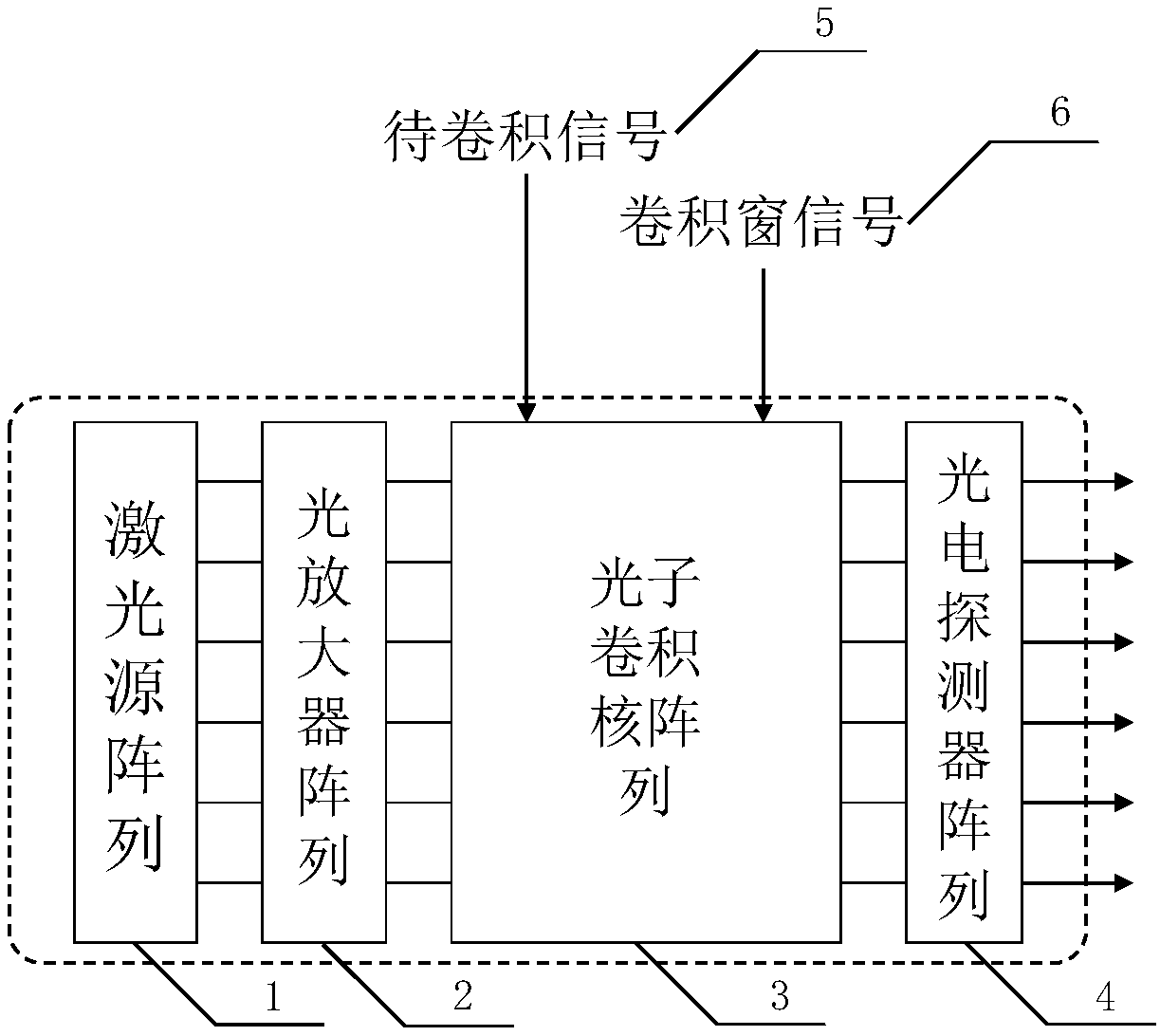
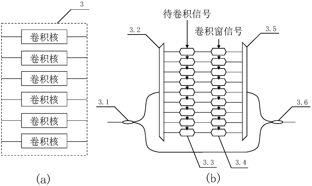
[0027] see figure 1 , figure 1 It is a diagram of an embodiment of the tiled photonic neural network convolution layer chip of the present invention. As can be seen from the figure, the tiled photonic neural network convolution layer chip of the present invention includes a laser source array 1, an optical amplifier array 2, a photon convolution kernel array 3 and a photodetector array 4, and the laser source array 1 has a total of M output terminals, the optical amplifier array 2 is composed of M input terminals, M optical amplifiers and M output terminals, the photon convolution kernel array 3 includes M photon convolution kernels of the same structure, the The photodetector array 4 comprises M photodetec...


PUM


Abstract

The invention discloses a tiled photon neural network convolution layer chip. The chip is universal for all the neutral network calculation including a convolution layer. To-be-operated data are represented in photonic integrated devices through light amplitude, a function of data operation is formed through cascaded connection and networking of the photonic integrated devices and an operation result is output in real time. By utilizing the adjustability of the photonic integrated devices, any signal can be modulated at the light amplitude, so that convolution calculation of any to-be-convoluted signal is realized. As the photonic information processing speed is at a constant level (that is velocity of light), the convolution calculation of a traditional computer framework can be increasedby multiple order magnitudes. Meanwhile, the tiled photon neural network convolution layer chip has a low energy consumption ratio.

Description

technical field [0001] The invention relates to intelligent photon signal processing technology and neural network technology, in particular to a photon neural network convolution layer chip technology. technical background [0002] Neural network is a classic machine learning algorithm, which is a computational model inspired by the neural information processing mode of the biological brain. Its proposal provides a more powerful and universal idea and method for human beings to solve machine learning problems. One of the typical applications is deep learning (Y. LeCun, et al, "Deep learning," Nature, vol.521, pp.436-444, 2015). Using multi-layer neural networks, deep learning can realize massive and complex data feature learning and provide intelligent prediction results with ultra-high accuracy. Its application fields are very wide. For example, in the field of computer graphics, deep learning has achieved breakthrough results in image recognition and classification, im...

Claims


Application Information

Patent Timeline
IPC IPC(8): G02B6/12G06E3/00
Inventor 邹卫文徐绍夫王静陈建平
Owner SHANGHAI JIAO TONG UNIV
Learn More