Transmission delay test method and device based on FPGA
A technology of transmission delay and test method, applied in the field of communication, can solve the problems of large safety margin of maximum transmission delay information, and FPGA chip cannot give full play to its performance, so as to reduce the design margin and improve the accuracy.
- Summary
- Abstract
- Description
- Claims
- Application Information
AI Technical Summary
Problems solved by technology
Method used
Image

Examples
Embodiment 1
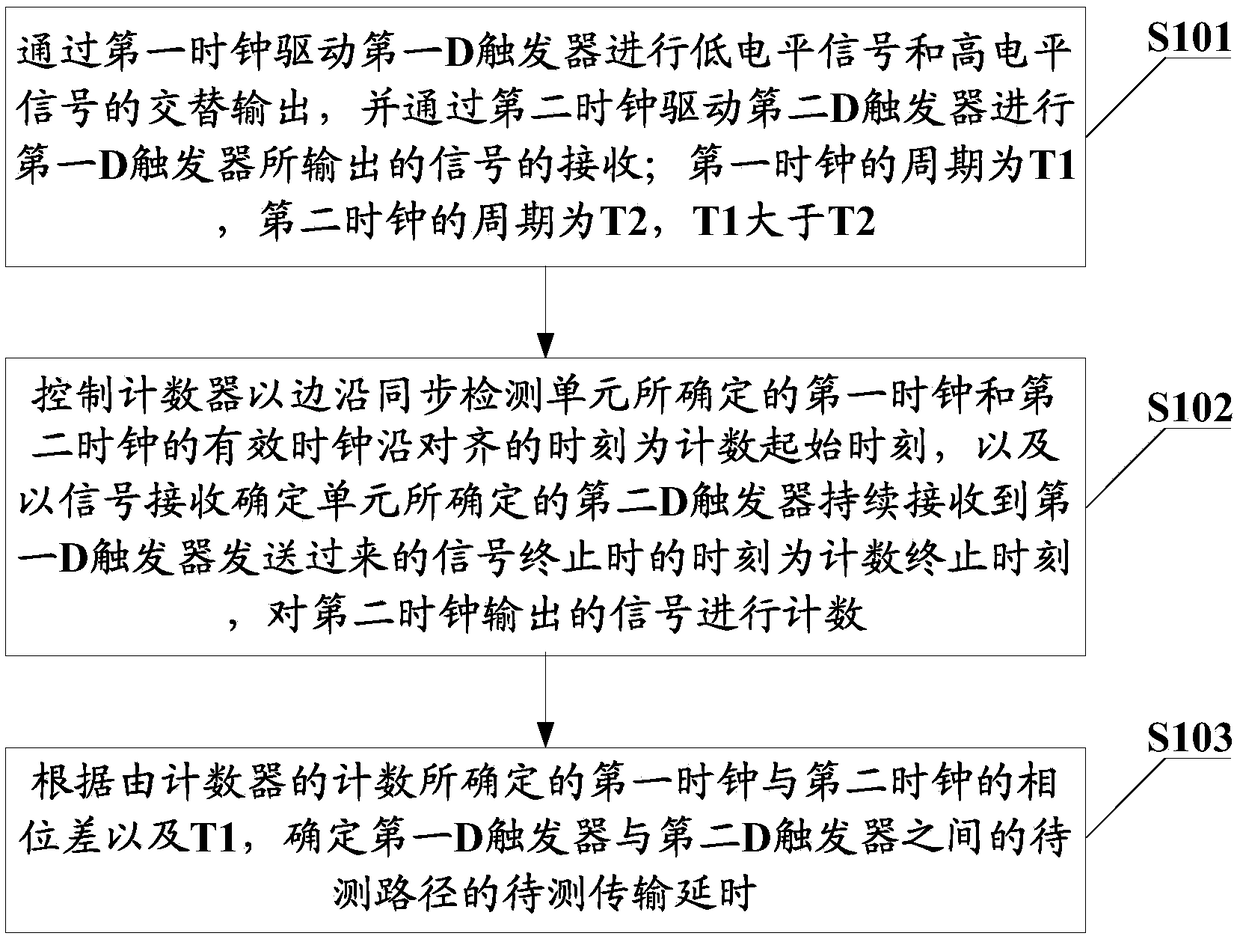
[0051] In order to solve the defect in the prior art that the maximum transmission delay information obtained by simulation based on the worst conditions has a larger safety margin than the actual one, which causes the FPGA chip to fail to fully utilize its performance, this embodiment provides a FPGA-based transmission delay test method, such as figure 1 Shown is the basic flowchart of the FPGA-based transmission delay testing method provided in this embodiment, and the transmission delay testing method specifically includes the following steps:
[0052] S101. Drive the first D flip-flop through the first clock to alternately output low-level signals and high-level signals, and drive the second D flip-flop through the second clock to receive signals output by the first D flip-flop; The period of the first clock is T1, the period of the second clock is T2, and T1 is greater than T2.
[0053] Specifically, in this embodiment, two clocks with different periods are input, and th...
Embodiment 2
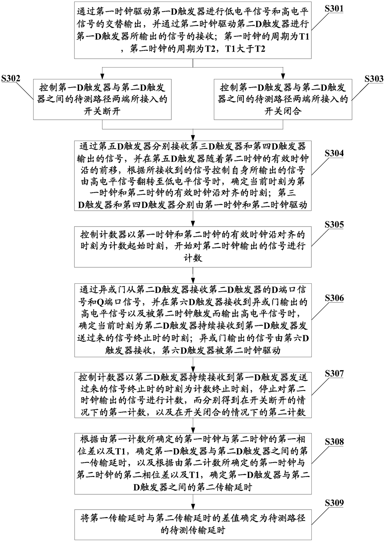
[0070] In order to better understand the present invention, the present embodiment illustrates the FPGA-based transmission delay testing method with a specific example, image 3 The detailed flowchart of the FPGA-based transmission delay test method provided by the second embodiment of the present invention, the transmission delay test method includes:
[0071] S301. Drive the first D flip-flop through the first clock to alternately output the low-level signal and the high-level signal, and drive the second D flip-flop through the second clock to receive the signal output by the first D flip-flop; The period of the first clock is T1, the period of the second clock is T2, and T1 is greater than T2.
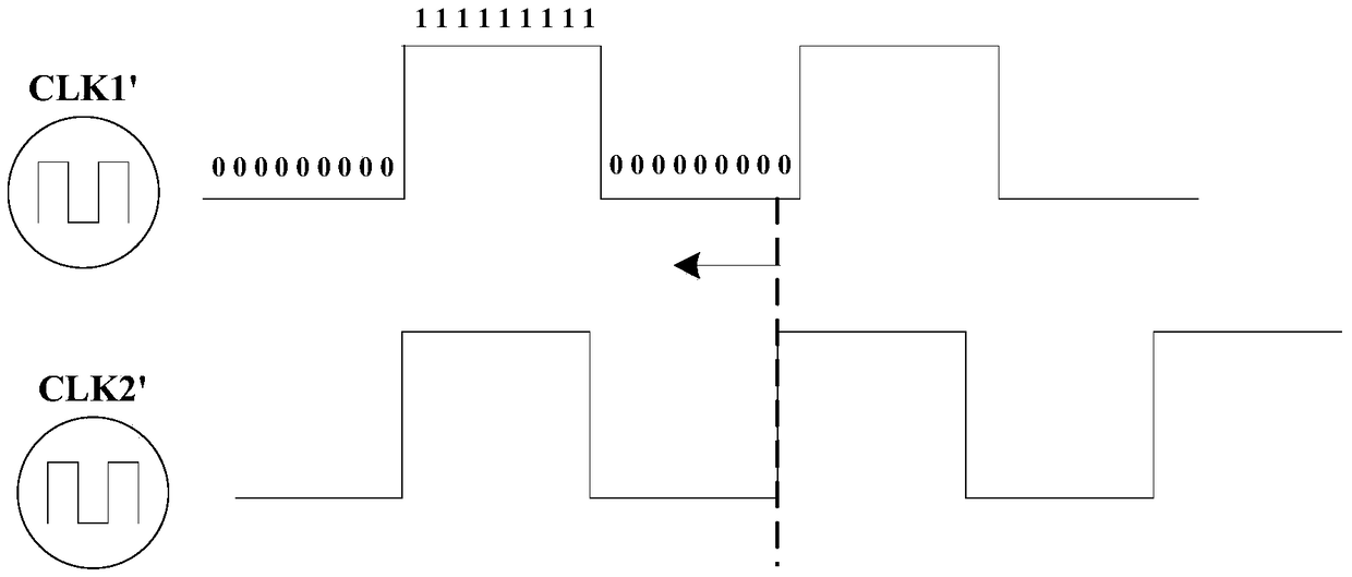
[0072] In this embodiment, two clocks with different periods are input, and the absolute value of the difference between the periods of these two clocks is also the transmission delay test accuracy in this embodiment, wherein the period T1 of the first clock CLK1 is relatively larg...
Embodiment 3
[0088] This embodiment provides a FPGA-based transmission delay testing device, for details, please refer to Figure 4 , including: a first clock 41, a second clock 42, a first D flip-flop 43, a second D flip-flop 44, a counter 45, an edge synchronization detection unit 46 and a signal reception determination unit 47, the first D flip-flop 43 and the second D flip-flop The path 48 to be tested is connected between the two D flip-flops 44; the Q port of the first D flip-flop 43 is connected back to the D port through an inverter, the cycle of the first clock 41 is T1, and the cycle of the second clock 42 is T2, T1 Greater than T2; the first clock 41 is used to drive the first D flip-flop 43 to alternately output low-level signals and high-level signals; the second clock 42 is used to drive the second D flip-flop 44 to perform the first D flip-flop 43 The reception of the output signal; the edge synchronous detection unit 46 is used to determine the moment when the effective clo...
PUM
 Abstract
Description
Claims
Application Information
 - R&D
- Intellectual Property
- Life Sciences
- Materials
- Tech Scout
- Unparalleled Data Quality
- Higher Quality Content
- 60% Fewer Hallucinations
Browse by: Latest US Patents, China's latest patents, Technical Efficacy Thesaurus, Application Domain, Technology Topic, Popular Technical Reports.
© 2025 PatSnap. All rights reserved.Legal|Privacy policy|Modern Slavery Act Transparency Statement|Sitemap|About US| Contact US: help@patsnap.com