Image sensor and manufacturing method thereof

A technology of an image sensor and a manufacturing method, which is applied to electric solid-state devices, semiconductor devices, radiation control devices, etc., can solve the problems of electron overflow, easy saturation of white light pixels, and degraded image quality, so as to improve sensitivity, reduce electronic crosstalk, and improve The effect of image quality

Active Publication Date: 2019-01-08
HUAIAN IMAGING DEVICE MFGR CORP
View PDF6 Cites 5 Cited by
  • Summary
  • Abstract
  • Description
  • Claims
  • Application Information

AI Technical Summary

Problems solved by technology

[0005] The technical problem to be solved by the technical solution of the present invention is to provide a new image sensor structure for the defect that the white light pixels in the existing image sensor are easily saturated, causing electrons to overflow into the adjacent photodiodes, thereby causing the image quality to decline Improving the imaging quality and imaging sensitivity of an image sensor under dark light and its manufacturing method

Method used


Image

  • Image sensor and manufacturing method thereof
  • Image sensor and manufacturing method thereof
  • Image sensor and manufacturing method thereof

Examples


Embodiment 1

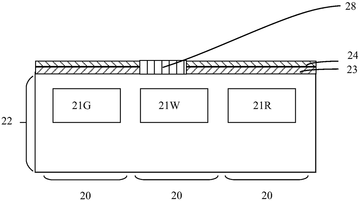
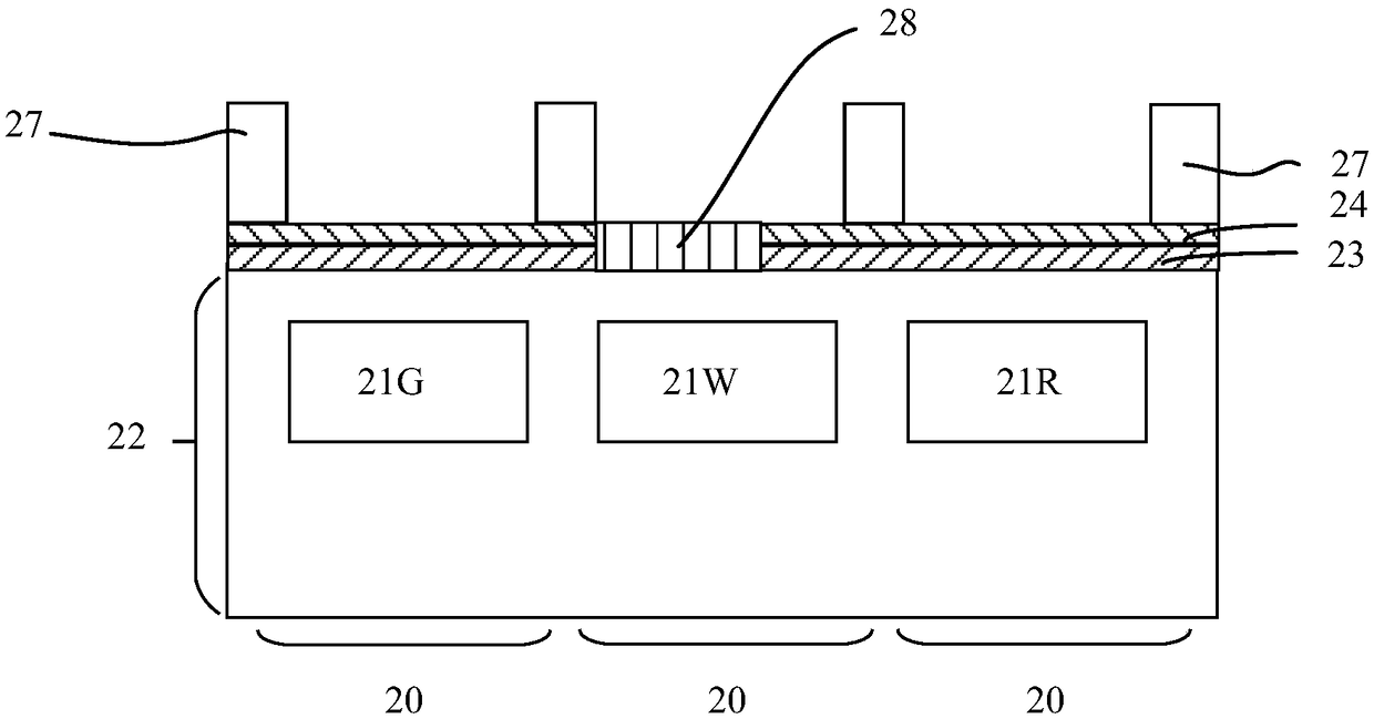
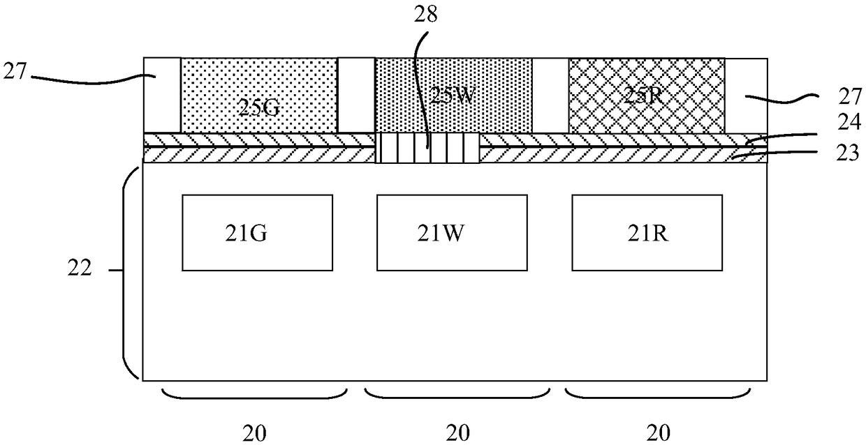
[0021] The manufacturing method of the image sensor in this embodiment includes: providing a semiconductor substrate 22 formed with a photodiode 21, the semiconductor substrate 22 includes different pixel regions 20, and the pixel region 20 includes a white pixel region; form an insulating structure on the insulating structure; form an organic photodiode 28 that penetrates the insulating structure and partially covers the white pixel region 20; forms a light-shielding film 27 that partially covers the insulating structure on the insulating structure; forms on the insulating structure Corresponding to the color filter layer 25 of different pixels, the color filter layer 25 includes a white color filter layer 25W, and the light-shielding film isolates the color filter layer 25 of the different pixels; it is formed above the color filter layer 25 at the corresponding position of each pixel area microlens26.

[0022] refer to figure 1 , first provide a semiconductor substrate 22...

Embodiment 2

[0045] refer to Figure 4 , In another embodiment of the present invention, another image sensor structure is provided, including: a semiconductor substrate 22 formed with photodiodes, the semiconductor substrate 22 includes different pixel regions 20, wherein the photodiodes correspond to different The pixel area includes a white pixel area; an insulating structure located on the semiconductor substrate; an organic photodiode 28 that penetrates through the insulating structure and partially covers the photodiode of the white pixel area; A light-shielding film 27 on the insulating structure and partially covering the insulating structure, the light-shielding film 27 isolating the different pixel regions 20; a color filter layer 25 corresponding to different pixels on the insulating structure, the color filter layer includes a white filter a color layer, the light-shielding film isolating the color filter layers of different pixels; and a microlens 26 located above the color fi...


PUM

PropertyMeasurementUnit
Thicknessaaaaaaaaaa

Abstract

The invention discloses an image sensor and a manufacturing method thereof. The image sensor comprises a semiconductor substrate formed with a photodiode, the semiconductor substrate comprises different pixel regions, and the pixel regions comprise white pixel regions. An insulating structure on the semiconductor substrate; An organic photodiode penetrating the insulating structure and partially covering the white pixel region photodiode; A light shielding film positioned on the insulating structure and partially covering the insulating structure; A color filter layer corresponding to different pixels on the insulating structure, wherein the color filter layer comprises a white color filter layer, and the light shielding film separates the color filter layers of the different pixels; A microlens located above the color filter layer. The image sensor not only improves the image quality of the image sensor, but also improves the sensitivity of the image sensor.

Description

technical field [0001] The invention relates to the field of manufacturing semiconductor devices, in particular to an image sensor and a manufacturing method thereof. Background technique [0002] An image sensor is a device that converts an optical image into an electrical signal. With the development of the computer and communication industries, the demand for high-performance image sensors is increasing. These high-performance image sensors are widely used in digital cameras, video recorders, personal communication systems (PCS), game consoles, security cameras, and medical miniature cameras. various fields. [0003] Image sensors are generally of two types, Charge Coupled Device (CCD) sensors and CMOS Image Sensors (CMOS Image Sensors, CIS). Compared with CCD image sensors, CMOS image sensors have the advantages of high integration, low power consumption, and low production cost. [0004] In the traditional CMOS photosensitive element, the photosensitive diode is loca...

Claims


Application Information

Patent Timeline
IPC IPC(8): H01L27/146
CPCH01L27/14603H01L27/14623H01L27/14643
Inventor 武海亮陈世杰黄晓橹
Owner HUAIAN IMAGING DEVICE MFGR CORP
Why Eureka
Try Eureka