Optical proximity correction method and mask making method

A technology of optical proximity correction and lithography mask, which is applied in the direction of optics, originals for photomechanical processing, photoplate making process of pattern surface, etc., can solve problems such as bridging damage, graphics missing corners, etc., and avoid electrostatic shock Wear, avoid graphics missing corners or bridge damage, reduce the effect of static electricity accumulation

Inactive Publication Date: 2018-12-25
HUAIAN IMAGING DEVICE MFGR CORP
View PDF6 Cites 8 Cited by
  • Summary
  • Abstract
  • Description
  • Claims
  • Application Information

AI Technical Summary

Problems solved by technology

[0005] However, in the mask pattern corresponding to the corrected pattern of optical proximity correction in the prior art, the phenomenon of missing corners or bridge damage is prone to occur at the opposite sharp feet of adjacent patterns.

Method used


Image

  • Optical proximity correction method and mask making method
  • Optical proximity correction method and mask making method
  • Optical proximity correction method and mask making method

Examples


Embodiment Construction

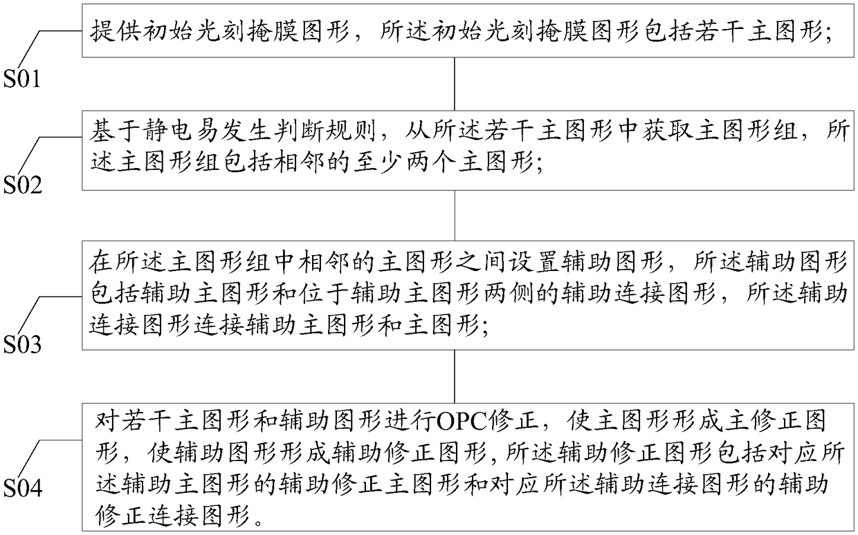
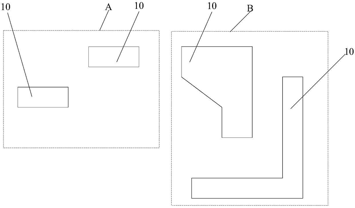
[0026] In the prior art, in the mask pattern corresponding to the corrected pattern of optical proximity correction, charges tend to accumulate at the opposite sharp feet of adjacent patterns to form a high electric field, thereby causing electrostatic breakdown, which in turn leads to the relative sharp feet of adjacent patterns The phenomenon of graphics missing corners or bridge damage occurs.

[0027] In order to avoid the phenomenon of graphic chipping or bridge damage at the opposite sharp feet of adjacent graphics, one method is to add an anti-static protective ring around the mask. The protection ring mainly plays a certain role in protecting the graphics on the periphery of the photomask. However, the protection ring has very little protection effect on the pattern positions where charge accumulation is likely to occur inside the photomask. For the graphics inside the mask, there will still be graphics chipping or bridge damage at the opposite sharp feet of adjacent ...


PUM


Abstract

An optical proximity correction method and a mask making method are provided. The optical proximity correction method includes: providing an initial photolithographic mask pattern including a plurality of main patterns; obtaining a main graphic group from a plurality of main graphics based on an electrostatic prone judgement rule, wherein the main graphic group comprises at least two adjacent maingraphics; setting auxiliary graphics between adjacent main graphics in the main graphics group, wherein the auxiliary graphics includes auxiliary main graphics and auxiliary connecting graphics on both sides of the auxiliary main graphics, and the auxiliary connecting graphics connect the auxiliary main graphics and the main graphics; performing OPC correction on the plurality of main graphics and auxiliary graphics to form main correction graphics from the main graphics and auxiliary correction graphics from the auxiliary graphics, wherein the auxiliary correction graphics comprise auxiliarycorrection main graphics corresponding to the auxiliary main graphics and auxiliary correction connection graphics corresponding to the auxiliary connection graphics. The optical proximity correctionmethod avoids the occurrence of graphic missing angles or bridging damage at opposite cusps of adjacent main correction graphics.

Description

technical field [0001] The invention relates to the field of semiconductor manufacturing, in particular to an optical proximity correction method and a mask plate manufacturing method. Background technique [0002] Photolithography technology is a crucial technology in semiconductor manufacturing technology. Photolithography technology can realize the transfer of graphics from the mask to the surface of the silicon wafer to form semiconductor products that meet the design requirements. The photolithography process includes an exposure step, a development step performed after the exposure step, and an etching step after the development step. In the exposure step, light is irradiated onto the silicon wafer coated with photoresist through the light-transmitting area of ​​the mask, and the photoresist reacts chemically under the irradiation of light; The photoresist is different to the degree of dissolution of the developer, forming a photoresist pattern, and realizing the tran...

Claims


Application Information

Patent Timeline
IPC IPC(8): G03F1/36
CPCG03F1/36
Inventor 徐一建梁凤云侯士权王婷倪凌云
Owner HUAIAN IMAGING DEVICE MFGR CORP
Why Eureka
Try Eureka